LTC4226 Parallel MOSFETs in Hot Swap Circuits
Introduction
While it is often desirable, and sometimes absolutely critical, to use multiple parallel MOSFETs in Hot Swap™ circuits, careful analysis of Safe Operating Area (SOA) is essential. Each additional parallel MOSFET added to a circuit improves the voltage drop, power loss, and accompanying temperature rise of the application. But, the parallel MOSFETs do not necessarily improve the transient power capability of the circuit. Unless every MOSFET is driven by an independent control loop, temporary high power events such as initial turn-on into a load or current limiting into a short circuit fault have a tendency to concentrate the power into a single MOSFET.
That being said, it is safe to connect MOSFETs in parallel to reduce the overall resistance using a single control loop as long as each MOSFET’s SOA is capable of withstanding the entire transient event.
The Good
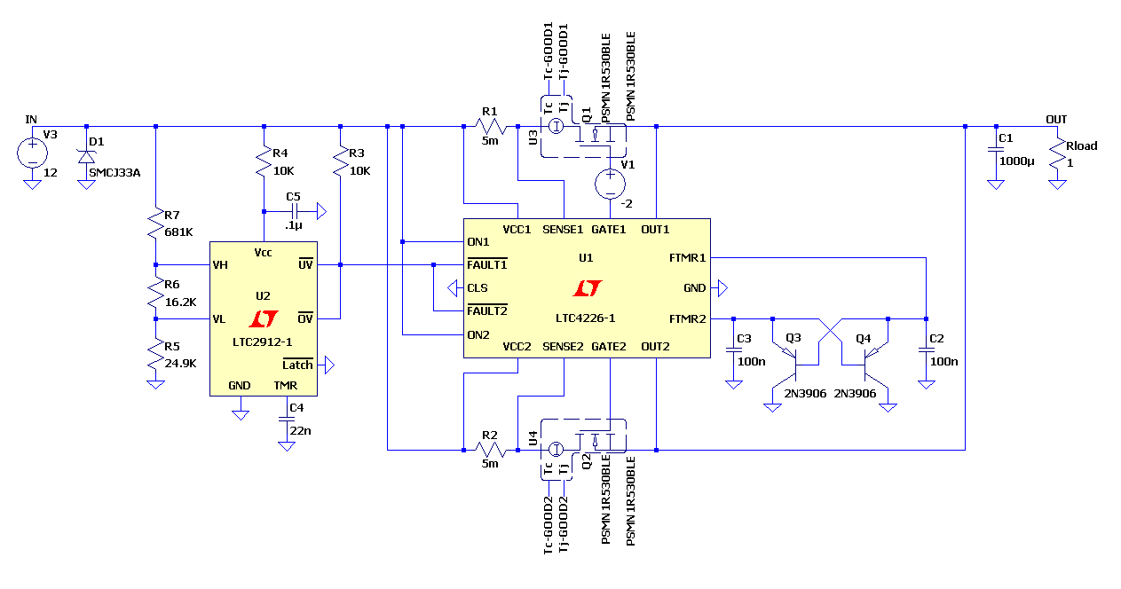
The Good SOA: Using Parallel MOSFETs with Independent Control Loops
A 12V/18A LTC4226 application circuit in the article MOSFET Safe Operating Area and Hot Swap Circuits uses two control loops to drive two MOSFETs. When you run the GOOD SOA simulation example in LTspice, the SOAtherm model verifies the SOA by indicating the MOSFET junction temperature. In this simulation, the worst case condition occurs at 1 second when the output is shorted to ground. A 2V voltage source is connected in series with one MOSFET’s gate to simulate threshold mismatch. (This represents the manufacturer’s process variation as well as the threshold shift induced by temperature mismatch and thermal runaway.) When you run the circuit simulation, you’ll see that the simulated MOSFET junction temperatures labeled Tj-GOOD1 and Tj-GOOD2 do not exceed the MOSFETs’ maximum rated junction temperature of 175°C.
The Good
The Bad
The Bad SOA: Parallel MOSFETs & Single Control Loop (9A instead of 18A)
The BAD SOA simulation example has two MOSFETs in parallel and a 5mΩ current sense resistor. Thus, the current limit is reduced to 9A compared to 18A above. The simulated MOSFET junction temperatures at nodes Tj-BAD1 and Tj-BAD2 indicate the same temperature as Tj-GOOD1 and Tj-GOOD2 in the first circuit. I chose to label these BAD not because the MOSFETs would be damaged, but because the first simulation makes full use of the SOA capabilities of the MOSFETs and is able to safely pass twice as much current to the load.
The Bad
The Ugly
The Ugly SOA: Parallel MOSFETs & Single Control Loop (Tj > 175°C)
Finally, the UGLY SOA simulation example shows two MOSFETs connected in parallel and driven by a single control loop instead of the two separate control loops in the first GOOD circuit. This time, one of the MOSFETs takes all of the power from the transient event at 1 second when the output is shorted to ground. It exceeds the 175°C maximum temperature of the MOSFET. In a real circuit, it is a matter of luck as to whether the MOSFETs survive this condition. If their thresholds match and they happen to share current equally, the circuit will appear to operate normally. But, on a bad day, one of the MOSFETs may start to take more power. As its temperature rises, its threshold drops and soon it hogs all of the power leaving none for the other MOSFET. On that day, things will clearly turn UGLY.
The Ugly
Conclusion
Good designers minimize solution cost and ensure that all MOSFETs are protected from exceeding their SOA limits. Bad designers spend more money than necessary by throwing away available SOA. But, it is the ugly designers that make the rest of us look good by creating the circuits that go up in smoke.
Recommendations for Further Reading:
- LTspice: SOAtherm Tutorial
- LTspice: Modeling Safe Operating Area Behavior of N-channel MOSFETs
- LTspice SOAtherm Support for PCB and Heat Sink Thermal Models
关于作者
他的职业生涯始于凌力尔特,设计了LTC2923和LTC2925电源跟踪控制器、LTC4355高压双通道理想二极管OR和LTC1546多协议收发器。他还是世界首款以太网供电控制器LTC4255的设计团队成员。他拥有两项与这些产品相关的专利。
随后,他搬到新加坡管理凌...


