∆Σ Breakthrough: LTC1966 True RMS-to-DC Converter Uses No Diodes, Heaters or Logarithms
∆Σ Breakthrough: LTC1966 True RMS-to-DC Converter Uses No Diodes, Heaters or Logarithms
2002-03-01
Introduction
The LTC1966 is a precision, micropower, true RMS-to-DC converter that utilizes an innovative patent-pending ∆Σ computational technique. The internal delta-sigma circuitry of the LTC1966 makes it simpler to use, more accurate, lower power and dramatically more flexible than conventional log-antilog RMS-to-DC converters. Unlike previously available RMS-to-DC converters, the superior linearity of the LTC1966 allows hassle-free system calibration at any input voltage.
The LTC1966 performance is summarized in Table 1. Unlike older log-antilog devices, the LTC1966 is insensitive to PC board soldering and stresses, as well as operating temperature. The LTC1966 is packaged in the space-saving MSOP package, which is ideal for portable applications. Additionally, the LTC1966 has an output impedance an order of magnitude higher than previous generation devices, so the averaging capacitor required is ten times smaller for the same design parameters, typically just 1μF. This is not trivial, because VOUT is a calculation node and cannot simply be decoupled by adding resistance.
| Parameter | Conditions | Value |
| Gain Accuracy | 50Hz to 1kHz | 0.1% |
| Total Error | 50Hz to 1kHz | 0.25% |
| Linearity | 0.02% | |
| Supply Current | 155μA Typ, 170μA Max | |
| Shutdown Current | 0.1μA | |
| Bandwidth | Independent of Input Voltage | 800kHz – 3dB, 6kHz±1% |
| Supply Range | Single Supply | 2.7V–5.5V |
| Dual Supply | ±5V |
The flexibility of the LTC1966 is illustrated in the typical applications shown in Figures 1 and 2. The LTC1966 accepts single ended or differential input signals (for EMI/RFI rejection) and supports crest factors up to 4. Common mode input range is rail-to-rail while the differential input range is 1VPEAK. The LTC1966 also has a rail-to-rail output with a separate output reference pin providing flexible level shifting. The LTC1966 operates on a single power supply from 2.7V to 5.5V or dual supplies up to ±5.5V. When the LTC1966 is shut-down, supply current is reduced to just 0.1μA.
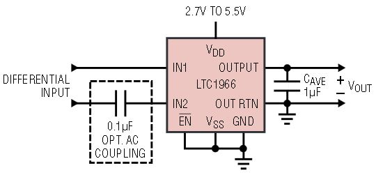
Figure 1. Single supply RMS-to-DC converter
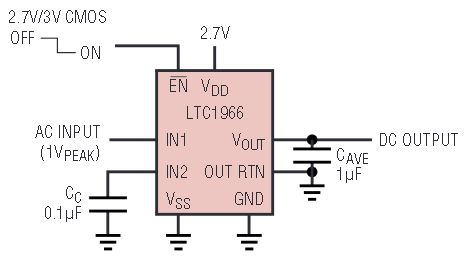
Figure 2a. 2.7V single supply, single ended, AC-coupled input RMS-to-DC converter with shutdown
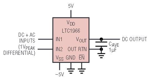
Figure 2b. ± 5V supplies, differential, DC-coupled inputs RMS-to-DC converter
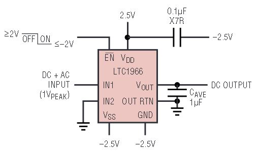
Figure 2c. ± 2.5V supplies, single ended, DC-coupled input RMS-to-DC converter
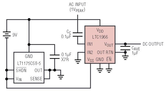
Figure 2d. Battery-powered RMS-to-DC converter with single-ended AC-coupled input
How an RMS-to-DC Converter Works
RMS amplitude is the consistent, fair and standard way to measure and compare dynamic signals of all shapes and sizes. Simply stated, the RMS amplitude is the heating potential of a dynamic waveform. A 1VRMS AC waveform will generate the same heat in a resistive load as will 1V DC. Mathematically, RMS is the “Root of the Mean of the Square:”

Monolithic RMS-to-DC converters use an implicit computation to calculate the RMS value of an input signal. The fundamental building block is an analog multiply/divide used as shown in Figure 3. Analysis of this topology is easy and starts by identifying the inputs and the output of the lowpass filter. The input to the LPF is the calculation from the multiplier/divider: (VIN)2/VOUT. The lowpass filter will take the average of this to create the output, mathematically:
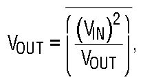
Because VOUT is DC,
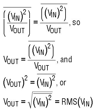
Note that this technique results in higher error at zero output signal because of the divide by zero.
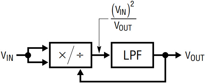
Figure 3. RMS-to-DC converter with implicit computation
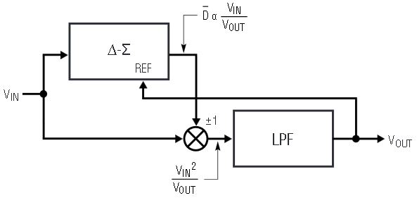
Figure 4. Topology of the LTC1966
Move Over Log-Antilog
Old RMS-to-DC converters used log-antilog techniques to perform the square and square-root analog mathematical functions. RMS-to-DC converters that use these techniques suffer from poor linearity, amplitude-dependent bandwidth and settling time, gain that drifts with temperature and other problems.
Figure 5 compares the linearity of the LTC1966 with that of the now obsolete log-antilog methods.
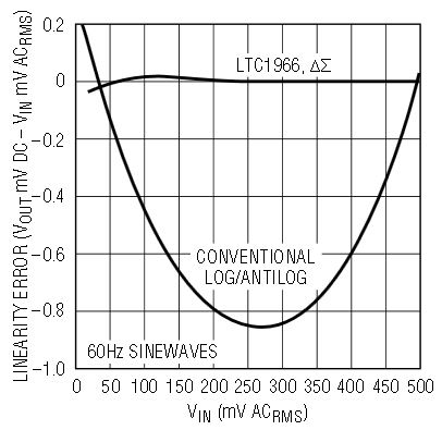
Figure 5. Linearity
How the LTC1966 RMS-to-DC Converter Works
The LTC1966 uses a similar topology but with a completely new implementation (see Figure 4). A ∆Σ modulator acts as the divider, and a simple polarity switch is used as the multiplier.
The ∆Σ is a 2nd order modulator with excellent linearity. It has a single-bit output whose average duty cycle is proportional to the ratio of the input signal divided by the output. The single-bit output is used to selectively buffer or invert the input signal. Again, this is a circuit with excellent linearity, because it operates at only two gains: –1 and +1. The average effective multiplication over time will be on the straight line between these two points.
Applying VOUT to the ∆Σ reference voltage results in the VIN2/VOUT function before the lowpass filter, and causes the RMS-to-DC conversion as was the case in Figure 3.
The lowpass filter performs the averaging of the RMS function and must be a lower corner frequency than the lowest frequency of interest. The LTC1966 needs only one capacitor on the output to implement the lowpass filter. The user selects this capacitor depending on frequency range and settling time requirements, and given the 85kΩ output impedance.
This topology is inherently more stable and linear than log/antilog implementations primarily because all of the signal processing occurs in circuits with high gain op amps operating closed loop. Note that the internal scalings are such that the ∆Σ output duty cycle is limited to 0% or 100% only when VIN exceeds ±4 • VOUT.
Linearity of an RMS-to-DC Converter
Linearity may seem like an odd property for a device that implements a function that includes two very non-linear processes: squaring and square rooting.
However, an RMS-to-DC converter has a transfer function, RMS volts in to DC volts out, that should ideally have a 1:1 characteristic. To the extent that the input to output transfer function is not a perfectly straight line, the part is nonlinear, and a source of error. Again, see Figure 4.
A more complete look at linearity uses the simple model shown in Figure 6. Here an ideal RMS core is corrupted by both input circuitry and output circuitry that have imperfect transfer functions.

Figure 6. Linearity model of an RMS-to-DC converter
Any nonlinearity that occurs in the output circuitry will corrupt the RMS in to DC out transfer function. A nonlinearity in the input circuitry will typically corrupt that transfer function far less simply because with an AC input, the RMS-to-DC conversion will average the nonlinearity from a whole range of input values together.
But the input nonlinearity will still cause problems in an RMS-to-DC converter because it will corrupt the accuracy as the input signal shape changes. Although an RMS-to-DC converter will convert any input waveform to a DC output, the accuracy is not necessarily as good for all waveforms as it is with sine waves. A common way to quantify dynamic signal wave shapes is Crest Factor. The crest factor is the ratio of the peak value relative to the RMS value of a waveform. A signal with a crest factor of 4, for instance, has a peak that is four times its RMS value. Because this peak has energy (proportional to voltage squared) that is 16 times (42) the energy of the RMS value, the peak is necessarily present for at most 6.25% (1/16) of the time.
The LTC1966 performs very well with crest factors of 4 or less, as shown in Figure 7. This excellent performance with crest factors less than 4 is directly attributable to the high linearity throughout the LTC1966. As shown in Figure 8, the LTC1966 will respond, but with reduced accuracy, to signals with higher crest factors. A crest factor greater than 4 is by definition a waveform with peaks less than 6.25% of the time.
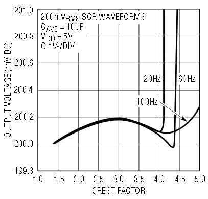
Figure 7. Performance vs crest factor
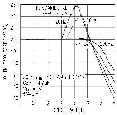
Figure 8. Performance vs large crest factors
Designing with the LTC1966
The LTC1966 RMS-to-DC converter makes it easy to implement a rather quirky function. For many applications all that will be needed is a single capacitor for averaging, appropriate selection of the I/O connections, and power supply bypassing.
The RMS or root-mean-squared value of a signal, the root of the mean of the square, cannot be computed without some averaging to obtain the mean function. The LTC1966 converter utilizes a single capacitor on the output to do the low frequency averaging required for RMS-to-DC conversion. A larger capacitor will allow RMS averaging of lower frequency inputs, but will result in longer settling time. The LTC1966 has a consistent settling time, dependent only on the averaging time constant and not on the input signal amplitude (unlike log-antilog RMS-to-DC approaches). The trade-offs between low frequency accuracy and settling time are thoroughly described in the Design Cookbook section of the LTC1966 datasheet, available at www.analog.com.
Conversion Bandwidth
As with any finite-bandwidth system, the LTC1966 will have increased errors with higher input frequencies. The LTC1966 is designed for high accuracy RMS-to-DC conversion of signals into and above the audible frequency range. The input sampling amplifiers have a –3dB frequency of 800kHz. However, the switched capacitor circuitry samples the inputs at a modest 100kHz. The output response versus frequency is shown in Figure 9.
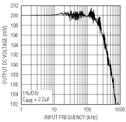
Figure 9. Input signal bandwidth
Although there is a pattern to the response versus frequency that repeats every sample frequency, the errors are not overwhelming. This is because LTC1966 RMS calculation is inherently wideband, operating properly with minimal oversampling, or even undersampling, using several proprietary techniques to exploit the fact that the RMS value of an aliased signal is the same as the RMS value of the original signal. However, a fundamental feature of the ∆Σ modulator is that sample estimation noise is shaped such that minimal noise occurs with input frequencies much less than the sampling frequency, but such noise peaks when input frequency reaches half the sampling frequency. Fortunately the LTC1966 output averaging filter greatly reduces this error, but the RMS-to-DC topology frequency shifts the noise to low (baseband) frequencies. So with input frequencies above 5kHz to 10kHz, the output will slowly wander around plus or minus a percent or so, as shown in Figure 9.
Interfacing with an ADC for a DVM
The LTC1966 output impedance and the low frequency RMS averaging ripple need to be considered when using an analog-to-digital converter (ADC) to digitize the LTC1966 RMS result.
The simplest configuration is to connect the LTC1966 directly to the input of a type 7106/7136 ADC as shown in Figure 10. These devices are designed specifically for DVM/DPM use and include display drivers for a 3½ digit LCD segmented display. Using a dual-slope conversion, the input is sampled over a long integration window, which results in rejection of line frequency ripple when integration time is an integer number of line cycles. Finally, these parts have an input impedance in the GΩ range, with specified input leakage of 10pA to 20pA. Such a leakage, combined with the LTC1966 output impedance, results in just 1μV to 2μV of additional output offset voltage.
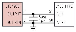
Figure 10. Interfacing to DVM/DPM ADC
Another type of ADC that has inherent rejection of RMS averaging ripple is an oversampling ∆Σ ADC such as the LTC2420. Its input impedance is 6.5MΩ, but only when it is sampling. Since this occurs only half the time at most, if it directly loads the LTC1966, a gain error of –0.54% to –0.73% results. In fact, the LTC2420 DC input current is not zero at 0V, but rather at one half its reference, so both an output offset and a gain error will result. These errors will vary from part to part, but with a specific LTC1966 and LTC2420 combination, the errors will be fixed, varying less than ±0.05% over temperature. So a system that has digital calibration can be quite accurate despite the nominal gain and offset errors. With 20 bits of resolution, this part is more accurate than the LTC1966, but the extra resolution is helpful because it reduces nonlinearity at the LSB transitions as a digital gain correction is made. Furthermore, its small size and ease of use make it attractive.
This connection is shown in Figure 11, where the LTC2420 is set to continuously convert by grounding the CS pin. The gain error will be less if CS is driven at a slower rate. Nevertheless, the rate should either be consistent or at a rate low enough that the LTC1966 and its output capacitor have fully settled by the beginning of each conversion, so that the loading errors are consistent.
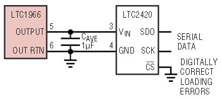
Figure 11. Interfacing to LTC2420
Applications
Single Supply Rumble Meter
Vibration and rumble in heavy industrial applications can give warning signs of impending equipment failure. Judicious monitoring of equipment vibration can indicate preventative maintenance is needed for worn or wearing parts, such as roller bearings, before catastrophe hits. Figure 12 shows how the LTC1966 simplifies this task. R1 and R2 bias up the LTC1966 inputs at mid supply, adding less than 3μA to the total supply current. Vibration energy at the geophone generates an AC voltage with approximately a 0.88V/inch/sec coefficient, and a frequency response of 10Hz to greater than 500 Hz. R3 is optional, providing low frequency damping. The LTC1966 performs an RMS-to-DC conversion on the vibration energy information and converts it into a simple more easily monitored DC output.
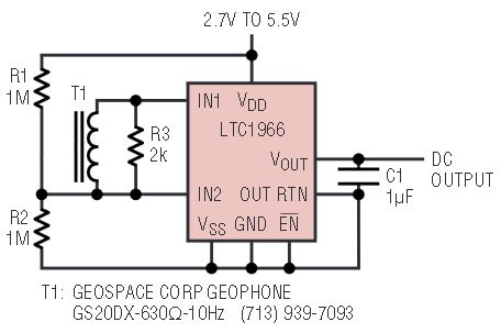
Figure 12. Single supply, micropower rumble/vibration meter
Audio Compressor
The last 30 years or so has seen a dramatic rise in the availability of consumer-ready, wide-dynamic-range audio. Typical modern movie material varies between explosions and whispers so frequently that the at-home audience is required to turn up the volume in order to hear the whispers, and during explosion sequences, turn down the volume in order to keep the kids in bed and maintain friendly relations with the neighbors. Figure 13 shows an audio frequency band compressor, which automatically amplifies the whispers and attenuates the explosions. The circuit uses the LTC1966 for the amplitude measurement, and applies feedback to adjust the effective gain of the LT1256 fader.
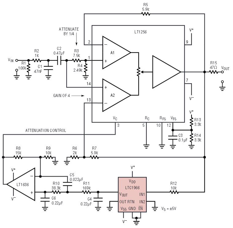
Figure 13. Audio amplitude range compressor
Resistors R2 through R4 and capacitors C1 and C2 form a simple 34Hz to 3.4kHz bandpass filter, with R1 merely providing a bleed path. Resistors R3 through R7 set the LT1256 amplifier paths A1 and A2 in gains of 1/4 and 4, respectively. The LTC1966 measures the output and adjusts the VC pin of the LT1256, through the LT1636 configured as a low pass filter, favoring the lower gain A1 path as output amplitude rises. It is this attenuating characteristic with rising output amplitude that achieves the compression effect.
As shown, the circuit provides 13dB of compression, squeezing a 5mV to 1VRMS input range into a 20mV to 0.85VRMS output range. Figure 14 shows results with a 16-fold step in input amplitude of a 100Hz sinusoid, demonstrating approximately 50ms of attack time. Note the presence of gain on the small signal, and the attenuation of the large signal. More extreme compression over different input and output ranges can be achieved by adjusting the op amp gain (R8 and R9), the fader gain and attenuation (R3 through R7), and the LT1256 full scale control voltage setting (R13 and R14). The upper limit on achievable compression is dictated by the desired quality of the time domain response of the control loop, with excessive overshoot on the attack time causing periods of excessive attenuation—creating a puffy sound to the human ear.
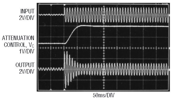
Figure 14. Response of compressor to a 16-fold amplitude step. Small signal is amplified and large signal is attenuated.
Summary
The LTC1966 is a breakthrough in RMS-to-DC conversion—bringing a new level of accuracy to RMS measurements. It is extremely simple to connect, and provides excellent accuracy over temperature and time without requiring trims. These features, along with its small size and micropower operation make the LTC1966 suitable for a wide range of RMS-to-DC applications, including handheld measurement devices.


