LTC1705: 2-Step Voltage Conversion Reduces Size and Heat in Notebook Computer Supply
LTC1705: 2-Step Voltage Conversion Reduces Size and Heat in Notebook Computer Supply
by
Haresh Patel
2001-12-01
Linear Technology’s LTC1705 is the most integrated CPU core, I/O and clock supply solution for Intel’s mobile Pentium® III microprocessor. This chip is a part of a “2-step” conversion architecture. 2-step conversion uses a primary regulator to convert the input power source (Li-Ion batteries) to 5V. This 5V supply is down-converted to provide a lower processor core voltage, I/O and clock supply by the LTC1705. Each regulator in a 2-step system maintains a relatively low step-down ratio (5:1 or less), running at high efficiency while maintaining a reasonable duty cycle (VO/VIN). In contrast, a single-step conversion from a high input voltage to a 1.xV output must operate at a very narrow duty cycle, mandating trade-offs in external component values while compromising efficiency and transient response.
2-step regulation can also buy advantages in thermal management. In a typical microprocessor core supply regulator, the DC/DC controller is located next to the CPU. In a 1-step design, all of the power dissipated by the core regulator is located next to the already hot CPU, making thermal management a nightmare. In a 2-step LTC1705 design, a significant percentage of the power lost in the core regulation system occurs in the 5V supply, which is usually located away from the CPU. The power lost to heat in the LTC1705 section of the system is relatively low, minimizing the added heat near the CPU. 2-step solutions using the LTC1705 usually match or exceed the total system efficiency of single-step solutions and provide the additional benefits of improved transient response, reduced PCB area and simplified power trace routing.
The LTC1705 uses a constant 550kHz switching frequency that allows the use of physically small inductors. The LTC1705 includes two switching regulator controllers, one for the CPU core and one for the I/O, each designed to drive a pair of N-channel MOSFETs in a voltage-mode feedback, synchronous buck configuration. An onboard 5-bit DAC sets the core output voltage according to the Intel mobile VID specification. The IC also includes a low dropout linear regulator (LDO) that delivers more than 150mA of output current for the CLK supply. The LTC1705 also has an open-drain PGOOD pin that indicates when all three outputs are within ±10% of their regulated values.
The circuit in Figure 1 is a typical Intel mobile Pentium III application for the core, I/O and clock supplies. The core voltage is VID controlled and can vary from 0.9V to 2.0V at 18A. The I/O voltage is set for 1.5V at 3A and is programmed by two resistors. The clock voltage is set internally for 2.5V at 150mA. Figure 2 shows the typical core efficiency for various output voltages and Figure 3 shows the core output transient response for a 14A load step.
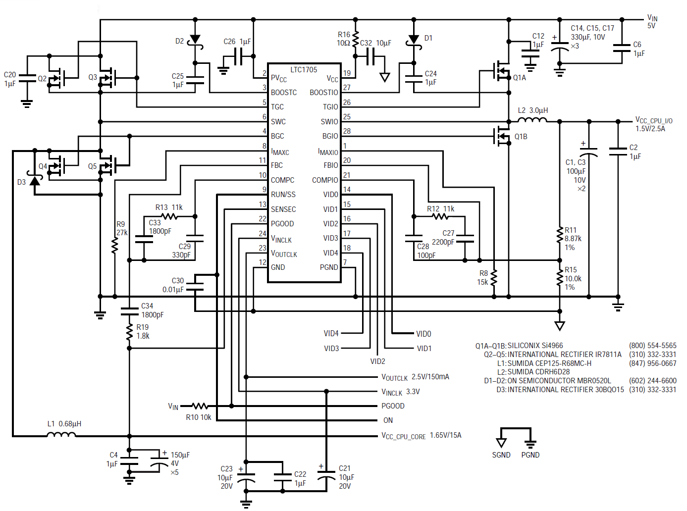
Figure 1. LTC1705 typical application for mobile Pentium III processor
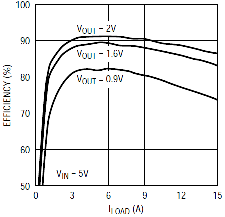
Figure 2. LTC1705 typical efficiency for various output voltages
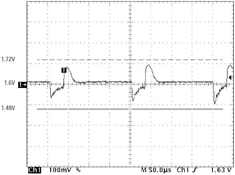
Figure 3. Transient response of Figure 1’s circuit for a 0A to 14A load step
LTC1705 Circuit with Active Voltage Positioning (AVP)
Figures 4 and 5 show two methods of implementing active voltage positioning on an LTC1705 circuit. In Figure 4, the voltage deregulation is set by adding a 2.5mΩ resistor (R18) in the power path. At full load, the output voltage will be less than nominal by IFULL LOAD • 0.0025. In order to program the output voltage higher than nominal at zero load, a 390k resistor (R17) is added between FB1 and ground. The DC value by which the output voltage increases over nominal can be calculated by the following formula:

where 0.8 is the feedback voltage and 10k is the top feedback resistor for the LT1705’s internal DAC.
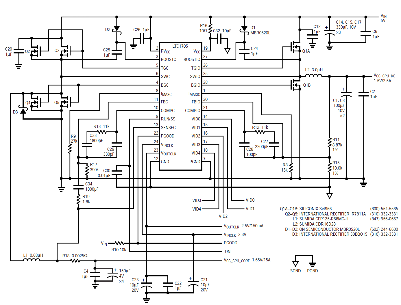
Figure 4. LTC1705 application with an external sense resistor for active voltage positioning
In Figure 5, the voltage deregulation is set by the DC resistance of the power inductor L1, which is approximately 2.5mΩ. The SENSE pin of the LTC1705 is connected between R20 (150Ω) and C24 (1µF). R20 and C24, which are connected across the inductor L2, act as a lowpass filter with a time constant of 150µs. Likewise, a 390k resistor is added between FB1 pin and ground. Figures 6 and 7 show the transient response of the LTC1705 circuits in Figures 4 and 5, respectively, for a 0A to 14A transient load step with four 150µF Sanyo POSCAP capacitors.
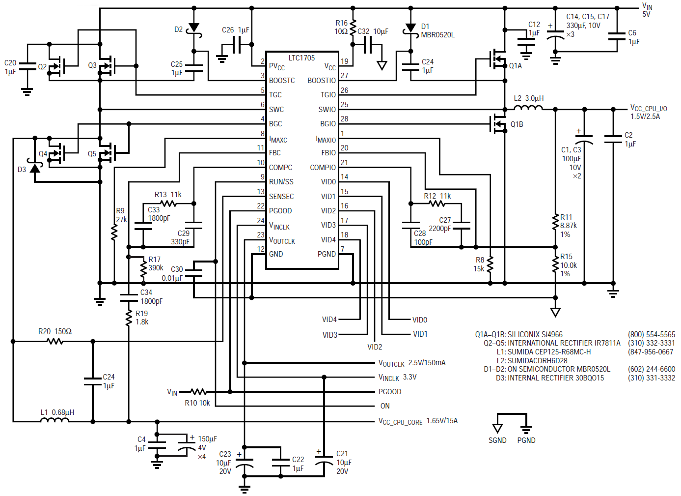
Figure 5. LTC1705 application that uses the resistance of the power inductor for active voltage positioning
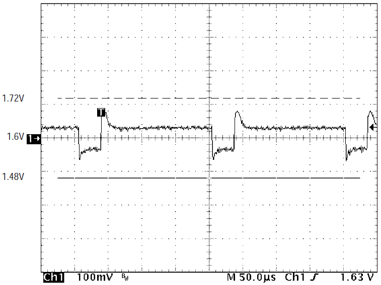
Figure 6. Transient response for Figure 4’s circuit with a 0A to 14A load step
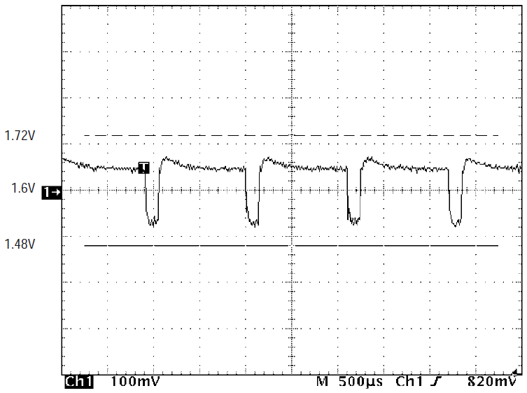
Figure 7. Transient response for Figure 5’s circuit with a 0A to 14A load step
Conclusion
The LTC1705 minimizes expensive bulk output capacitors by using active voltage positioning (AVP). It also takes advantage of 2-step conversion and the produces the most efficient and highly integrated CPU Core, I/O and clock supply currently available for Intel’s mobile Pentium III microprocessor.
Pentium is a registered trademark of Intel Corporation.


