The LTC1625 Current Mode DC/DC Controller Eliminates the Sense Resistor
Introduction
Power supply designers have a new tool in their quest for ever higher efficiencies. In the past, when designing a step-down DC/DC converter, one had to choose between the high efficiency of voltage mode control and the many benefits of current mode control. Although voltage mode control offers high efficiency and a simple topology, it is difficult to compensate, has poor rejection of input-voltage transients and does not inherently limit output current under fault conditions, such as an output short circuit. Current mode control overcomes these problems by adding a control loop to regulate the inductor current in addition to the output voltage. Unfortunately, a sense resistor is required to measure this current, which adds cost and complexity while reducing converter efficiency. However, with the new LTC1625 No RSENSE™ controller, one can enjoy all of the benefits of current mode control without the penalties of using a sense resistor.
The LTC1625 is a step-down DC/DC switching regulator controller that incorporates popular features from the LTC1435 and related parts. It is capable of a wide range of operation with inputs from 3.7V to 36V. Fixed output voltages of 5V and 3.3V can be selected or an external resistive divider can be used to obtain output voltages from 1.19V up to nearly the full input voltage. The controller provides synchronous drive for N-channel power MOSFETs and retains the advantage of low dropout operation typically associated with P-channel MOSFETs. Burst Mode™ operation maintains efficiency at low load currents, but can be overridden to assist secondary-winding regulation by forcing continuous operation. In addition to eliminating the sense resistor, the LTC1625 further reduces the external parts count by incorporating the oscillator timing capacitor. The oscillator frequency can be set to 150kHz, 225kHz, or can be injection locked to any frequency between these points.
Current Mode Control without a Sense Resistor
How does one implement current mode control without a current sense resistor? The answer is to make the standard power MOSFET switches do double duty as current sense elements. By measuring the drain-to-source voltage of a MOSFET operating in the triode region, one can use the RDS(ON) of the device as a sense resistance. Although conceptually simple, this is tricky to implement in practice because inductor current information can only be obtained when a MOSFET is turned on. Figure 1 illustrates how this is accomplished in the LTC1625. The drain-to-source voltages of the power MOSFETs are sensed through the TK, SW and PGND pins. Sense amplifiers TA and BA measure and amplify these voltages only when the respective MOSFET is conducting current. The two resulting signals (VT and VB) are summed to create a sense voltage ramp (VS) that is proportional to the inductor current throughout the entire switching cycle. A current comparator (I) uses the sense voltage and a current threshold voltage (ITH) to control the power MOSFETs. Because the LTC1625 fully recovers the inductor current information, it behaves identically to traditional current mode controllers that use a sense resistor.

Figure 1. The LTC1625 senses VDS across the power MOSFETs to infer inductor current.
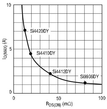
An important feature of current mode control is its ability to inherently limit load current simply by restricting the range of the current-threshold voltage. The maximum allowed current is then inversely proportional to the sense resistance. With the LTC1625, the power MOSFET on-resistance determines the maximum output current. An approximate graph of this relationship is shown in Figure 2, along with data points for some popular Siliconix MOSFETs. The on-resistance is typically guaranteed to be below a maximum specified by the manufacturer, but it will vary substantially between lots and over temperature. Thus, a design accommodating the maximum possible on-resistance will have a significantly higher maximum output current when this resistance is lower than normal. To ensure reasonable current levels in case of a fault, such as an output short to ground, the LTC1625 will fold back the current if the output voltage falls significantly.

Figure 2. Maximum output current is determined primarily by the on-resistance of the power MOSFETs.
Easing the Layout Challenge
Ensuring that switching transients do not interfere with the control loop is a common difficulty with high output-current power converters. A great deal of effort is often expended in board layout and component placement to subdue coupling effects, such as pulse pairing or grouping. Eliminating the sense resistor and its associated signal lines makes this job easier. In addition, the LTC1625 uses some internal blanking around the switching transitions to further reduce the possibility of jitter or pulse pairing in the control loop. The result is a controller that is relatively immune to these coupling effects and remarkably easy to lay out successfully. On the other hand, the addition of blanking increases the minimum time in which the controller can turn the top MOSFET on and off. This places a limit on the minimum duty cycle but does not unduly restrict the maximum input voltage for a given output voltage. Table 1 shows the many common input and output voltage combinations that the LTC1625 can accommodate.
| VOUT (V) | VIN (V) | ||||
| 5 | 12 | 18 | 24 | 30 | |
| 1.5 | ✓ | ✓ | |||
| 1.8 | ✓ | ✓ | ✓ | ||
| 2.5 | ✓ | ✓ | ✓ | ✓ | |
| 3.3 | ✓ | ✓ | ✓ | ✓ | ✓ |
| 5.0 | ✓ | ✓ | ✓ | ✓ | |
| 12.0 | ✓ | ✓ | ✓ | ||
Additional Features
The LTC1625 controller is designed for synchronous, step-down applications with two N-channel power MOSFETs. Using an N-channel MOSFET for the topside switch is more cost-effective than using a P-channel device, but it requires a floating topside driver. This driver is powered using an external bootstrap capacitor and diode. If the input voltage drops close to the output voltage, the LTC1625 will begin skipping cycles, leaving the top MOSFET on longer in order to maintain low dropout operation. Once in dropout, the boost capacitor is recharged by turning off the top MOSFET and turning on the bottom MOSFET briefly every tenth cycle. This maintains a duty cycle greater than 99% in dropout.
Another external part was eliminated by incorporating the oscillator timing capacitor into the LTC1625. The controller runs at a nominal 150kHz frequency that can be increased 50% by taking the SYNC pin above 1.2V. Frequency-sensitive applications can synchronize the oscillator by applying a clock signal between 165kHz and 200kHz to this pin.
Providing gate charge to the power MOSFET switches is one of the main sources of efficiency loss in switching regulators. The LTC1625 includes two features to minimize this loss. Normally, both MOSFETs are turned on and off once per oscillator cycle. When the load current drops to near zero, the gate charge required for switching becomes a significant fraction of the total input current. The LTC1625 addresses this problem with Burst Mode operation. As the load current decreases below approximately one fifth of its maximum value, both MOSFETs are turned off for a few cycles while the output capacitors support the load. In this way, gate charge is saved at the expense of fixed frequency operation. For applications that require it, fixed frequency operation can be maintained by tying the FCB pin low to force continuous operation at low load currents. This pin can also be used to adaptively override Burst Mode operation when regulating the output of a secondary winding. Another problem with gate charge is that it is normally drawn from the high voltage input supply. However, power can be saved by obtaining the gate charge from a high efficiency external supply (between 5V and 7V) connected to the EXTVCC pin. This could be the output voltage of the regulator, a boosted version of the output or some other system supply, if available.
Removing Output Voltage Constraints along with RSENSE
The LTC1625 can be configured for a wide variety of output voltages using the VPROG and VOSENSE pins. For basic 3.3V and 5V applications, one can use an internal resistive divider with the output connected directly to the VOSENSE pin. Connect the VPROG pin to INTVCC for a 5V output or to ground for a 3.3V output. Leaving the VPROG pin open disables the internal resistive divider and connects the error-amplifier feedback node directly to the VOSENSE pin. With an external resistive divider, the LTC1625 is capable of regulating an output voltage anywhere between the input voltage and the 1.19V internal reference. This represents a significant improvement over previous current mode controllers, which were constrained by the common mode range of the current sense signal lines.
Start-up and shutdown of the LTC1625 can be controlled via the RUN/SS pin. This pin is connected to an external capacitor that is charged from an internal 3µA current source. The controller will be shut down if this pin is held below 1.4V. After the pin is released, the part stays shut down while the capacitor is charged, permitting a controlled delay for sequencing the power supply start-up. When the voltage rises above 1.4V, the controller will start but with a clamp on the current threshold voltage that limits the load current to approximately one third of its maximum value. Limiting the load current reduces the inrush current into the converter. As the voltage increases above 1.4V, the clamp is gradually raised to its normal value.
Design Examples
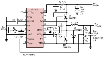
Figure 3 shows the LTC1625 in an application supplying a 2.5V output using an external feedback divider. Si4410DY MOSFETs from Siliconix allow this converter to deliver up to 5A of load current. Ripple current is 1.8A (36% of full load) and current limit occurs around 6A. Note also that the EXTVCC pin is connected to an external 5V supply. This increases efficiency by drawing the roughly 7mA gate charge current from a supply lower than VIN.

Figure 3. 2.5V/5A adjustable-output supply.
An efficiency plot of this circuit is shown in Figure 4. An LTC1435 with identical components in the power path is also plotted for comparison. At lower output voltages such as this, the sense resistor is responsible for an increasing share of the total power loss. By eliminating this source of loss, the LTC1625 is easily able to deliver an efficiency greater than 90% at high load current. The benefit of reduced I2R loss is readily apparent at the highest loads. The controller makes a transition to Burst Mode operation below around 1.1 A which keeps the efficiency high at moderate loads.

Figure 4. Efficiency vs load current.
A circuit demonstrating the wide output range of the LTC1625 is shown in Figure 5. This application uses Si4412DY MOSFETs to deliver a 12V output at up to 2.2A. Note that the SYNC pin is tied high for 225kHz operation in order to reduce the inductor size and ripple current.

Figure 5. 12V/2.2A adjustable-output supply.
Conclusion
The LTC1625 step-down DC/DC controller offers true current mode control without the expense and difficulty of using a sense resistor. Popular features from Linear Technology’s other controllers, such as fixed frequency operation, N-channel MOSFET drive, Burst Mode operation, soft-start and output voltage programming make this controller useful in a variety of applications. By eliminating the power loss in the sense resistor, even higher efficiencies can be achieved than were previously possible, making the LTC1625 an excellent choice for DC/DC converter designs requiring the highest performance.


