LT1766: 1.5A Converter Runs Directly from 60V DC
Introduction
With a maximum input voltage capability of 60V and peak switch current of 1.5A, the LT1766 is targeted for high voltage, industrial and automotive applications. The 60V maximum operating input voltage makes the LT1766 ideal for 12V, 24V and (future) 42V automotive systems, which must survive load-dump input transients as high as 60V. At high input-to-output voltage differentials, power dissipation is minimized by providing very fast switch edge rates and by sing a BIAS pin connected to the regulated output to supply internal control circuitry. At low input-to-output voltage differentials, a supply-boost capacitor is used to fully saturate an internal 200mΩ power switch to reduce DC switch losses. The LT1766 runs at a fixed frequency of 200kHz and can be externally synchronized. In addition, a pin is provided for programming undervoltage lockout and placing the part into micropower shutdown. The LT1766 maintains the 1.5A peak switch current over the full duty cycle range. This is achieved by the use of patented circuitry that cancels the effect of slope compensation on peak switch current without affecting frequency compensation.
The LT1766 is packaged in a 16-pin SSOP (GN-16) package, which occupies the same space as an SO-8 package. The LT1766 provides a wide range of functions, such as undervoltage lockout and micropower shutdown, along with external synchronization capability, without sacrificing the power saving features of a BIAS or BOOST pin. Also, the GN-16 package, with its fused corner pins, improves thermal performance, reducing the θJA of the package from 120°C/W (typical SO-8) to 95°C/W.
Circuit Description
The LT1766 is optimized to provide high efficiency for both high and low input-to-output voltage differentials in a buck-mode switching regulator topology. The block diagram in Figure 1 shows all of the key functions of the LT1766 step-down converter. A current mode architecture is used to provide fast transient response and good loop stability. Two feedback loops exist to control the duty cycle of the power switch using a transconductance error amplifier and a current sense comparator that monitors switch current on a cycle-by-cycle basis. Nonlinear slope compensation has been added to the current sense signal to prevent the subharmonic oscillation associated with current mode control when the regulator duty cycle is greater than 50%. An added feature of the LT1766, referred to as “anti-slope compensation” in the block diagram, eliminates the effects of slope compensation on the peak switch current at high duty cycles without affecting the frequency compensation. For high duty cycle applications, this is a significant benefit over competing current mode converters with similar peak switch current limits.
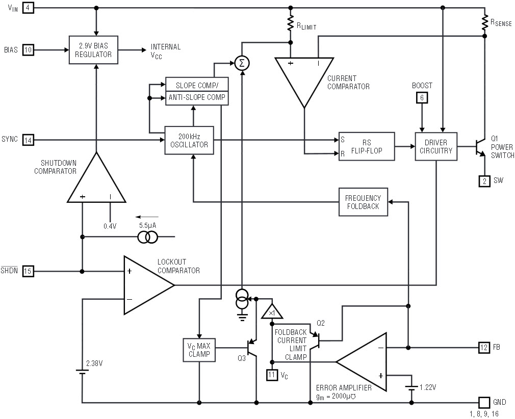
Figure 1. LT1766 block diagram.
The LT1766 also includes an accurate 1.2V reference. This reference is scaled to provide an accurate 2.38V threshold on the SHDN pin, allowing programming of undervoltage lockout; a second, lower threshold (0.4V) allows shutdown with the input supply current reduced to 25µA. The part can be externally synchronized to frequencies up to 700kHz.
LT1766 Features
The LT1766 provides the following features:
- Wide input range: 5.5V to 60V
- Constant 200kHz switching frequency
- 1.5A peak switch current
- 0.2Ω saturating switch
- Peak switch current maintained over full duty cycle range
- 25µA shutdown current
- 1.2V feedback reference
- Easily synchronizable
42V to 5V Buck Converter
The LT1766 was designed to address the need for high efficiency over a wide range of input voltages. A typical high input voltage application, a 42V to 5V converter, is shown in Figure 2a. To achieve high efficiency at high input voltages, fast output-switch edge rates are required; the LT1766 achieves edge rates of 1.2V/ns (rise) and 1.7V/ns (fall). In addition, light loads at high input voltages require minimal quiescent current to be drawn from the input. A BIAS pin allows the internal control circuitry to be supplied from the regulated output if greater than 3V. At a duty cycle of 12%, for example, this technique reduces input quiescent current from 4.5mA to approximately 1.8mA. The efficiency for a 42V to 5V conversion (>80%) is shown in Figure 2b.
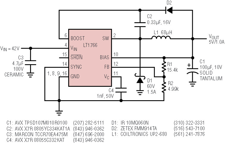
Figure 2a. 42V to 5V step-down converter.
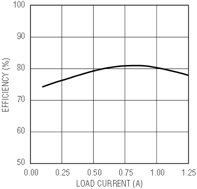
Figure 2b. Efficiency vs load current for Figure 2a’s circuit.
12V to 5V Converter
The LT1766 is capable of excellent efficiencies at lower input voltages; combined with its ability to withstand voltage transients up to 60V, this makes it ideal for power conversion in harsh environments such as automotive electronics. A typical 12V to 5V converter is shown in Figure 3a. The key to achieving high efficiency for low input-to-output voltage conversions is to use a saturating switch design. A prebiased capacitor, connected between the BOOST and SW pins, generates a boost voltage above the input supply during switching. Prebias is derived via a diode, D2, from the regulated output. Driving the switch from this boost voltage allows the 200mΩ power switch to fully saturate. The worst-case minimum BOOST voltage required to fully saturate the internal power switch is 3V above input supply. This means that an output voltage as low as 3.3V is ideal for prebiasing of the boost supply capacitor via a simple diode. The efficiency for a 12V to 5V conversion, which peaks at 90%, is shown in Figure 3b.
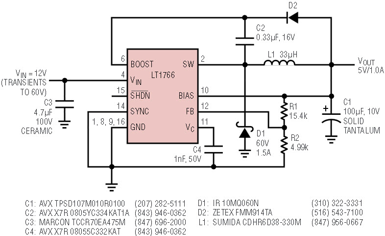
Figure 3a. 12V to 5V step-down converter.
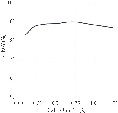
Figure 3b. Efficiency vs load current for Figure 3a’s circuit.
Conclusion
Having a peak switch current of 1.5A and a maximum input voltage capability of 60V, the LT1766 provides an ideal solution for 12V, 24V or (future) 42V automotive electronics in addition to 48V nonisolated telecom applications, where input voltages as high as 60V must be accommodated. Packaged in a 16-pin SSOP (GN16), which occupies the same space as an SO-8, and running at a fixed frequency of 200kHz, the LT1766 provides a compact solution for high voltage step-down power conversions.


