It Just Got Easier to Convert Lithium-Ion Battery Voltage to 3.3V with this Efficient Single Inductor Synchronous Buck-Boost Regulator
It Just Got Easier to Convert Lithium-Ion Battery Voltage to 3.3V with this Efficient Single Inductor Synchronous Buck-Boost Regulator
by
Mark Jordan
2002-03-01
Introduction
One of the most common power supply problems with today’s portable devices is generating a regulated voltage that falls some where in the middle of the full voltage range of the battery. For instance, providing a consistent 3.3V output from a Lithium-Ion (Li-Ion) battery’s range of 2.5V to 4.2V. The most popular topology for solving this problem is a SEPIC converter, but a SEPIC has some inherent drawbacks, including mediocre efficiency, and the requirement of both a coupled inductor and a high current flyback capacitor. Another solution is a circuit that cascades a boost converter with either an LDO or a Buck converter, but this relatively inefficient circuit doesn’t fare much better with the additional space and money it takes for the extra components. Analog Devices now offers another, better solution with the new LTC3440 Buck-Boost converter, which provides the most compact and highest efficiency solution yet—reducing cost, increasing battery life, and saving precious PC board real estate.
The LTC3440 is the industry’s first constant frequency, single inductor, buck-boost converter. The IC incorporates a patent pending control technique to efficiently regulate an output voltage above, below or equal to an input source voltage with only a single inductor, and without the requirement of Schottky diodes. Figure 1 shows the power stages of the topologies mentioned above—SEPIC, cascaded boost-buck and cascaded boost-LDO—and the single inductor topology using the LTC3440.

Figure 1. Various power stage topologies for Lithium-Ion to 3.3V conversion
Figure 2 shows the efficiencies for each topology versus input voltage. The LTC3440 solution is the only one of the group that can reach 95% efficiency, and maintain better than 90% efficiency across the entire operating voltage range of the battery.

Figure 2. Efficiency vs input voltage for the topologies in Figure 1
Features
The LTC3440’s input and output voltage ranges are both 2.5V to 5.5V. High frequency, low noise and high efficiency operation are due in part to low RDS(ON) (0.19Ω NMOS, 0.22Ω PMOS), low gate charge synchronous switches, and minimal break-before-make times. The LTC3440 is housed in a thermally enhanced MS10 package, which makes it ideal for portable power applications requiring less than two watts of output power.
To improve efficiency at light loads, the LTC3440 offers Burst Mode® operation, which draws only 25µA of quiescent current, further improving battery life. To enable Burst Mode operation, simply drive the MODE/SYNC pin high. Or, for noise-sensitive applications, drive the MODE/SYNC low to enable fixed frequency switching. The operating frequency can be programmed from 300kHz to 2MHz by changing the value of the resistor between the RT pin and ground. No external clock is required, though users can synchronize the operating frequency by connecting an external clock to the MODE/SYNC pin. The part can also be commanded to shutdown by pulling the SHDN/SS pin low. In shutdown, the part draws less than 1µA of quiescent current and disconnects the output from the input supply. To limit inrush current at start-up, connect an external RC network to the SHDN/SS pin to soft-start the output voltage.
LTC3440 Architecture
The topology incorporated in the LTC3440 (see the partial schematic shown in Figure 3) allows the regulator to smoothly transition from Buck mode to Buck-Boost mode, and then to Boost mode by properly phasing four output switches (SW A, SW B, SW C and SW D) in response to the error amp output voltage (VC pin). Since the error amp output voltage is a filtered signal, the duty cycle/mode control is insensitive to switching noise.
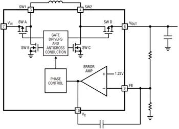
Figure 3. Detailed schematic of the LTC3440 output stage
Figure 4 shows each switch’s on-time as a function of the VC voltage. During Buck mode, switches A and B synchronously switch while D is on, and C is off. At the other extreme, when the regulator is in Boost mode, switches C and D synchronously switch, while A is on, and B is off. During the Buck-Boost mode, the input voltage approaches the output voltage, and all four switches commutate.

Figure 4. On-time of the output switches as a function of the error amp control voltage, VC
2-Watt, Li-Ion to 3.3V Converter
Figure 5 shows an all-ceramic capacitor,Lithium-Ion to 3.3V at 600mA application, which runs at 1MHz. Figure 6 shows the efficiency curves over the Li-Ion battery range. During decreased load demand, the converter can be commanded to enter power saving Burst Mode operation. With Burst Mode operation enabled at light loads, this design produces efficiencies of over 80% for more than two decades of load current. At 200µA of load current, the efficiency remains above 70%, primarily due to the low 25µA quiescent current. To provide inrush current limiting, add a resistor between from SHDN/SS and VIN and a capacitor between SHDN/SS and GND to limit the error amp output voltage rise time at start-up.

Figure 5. Simple Lithium-Ion to 3.3V converter at two watts

Figure 6. Efficiency of the circuit in Figure 5
3-Cell to 3.3V Converter at 600mA
The LTC3440’s architecture makes it useful for more than just Li-Ion applications. The LTC3440 is an ideal fit in 3-cell applications where the input voltage typically changes from 2.7V to 4.5V. Figure 7 shows a 3-cell to 3.3V application, with its efficiency curves shown in Figure 8. The switching frequency is programmed for 1.5MHz, so a smaller inductor can be used, allowing a faster transient response. Due to the higher frequency, Schottky diodes are added to obtain the maximum efficiency (2% typical at 1.5MHz). Type III error amp compensation (two pole, two zero) was utilized to maximize bandwidth, optimizing the transient response. This application also takes advantage of the soft-start feature for inrush current control.

Figure 7. 3-cell to 3.3V at 600mA with optional Schottky diodes

Figure 8. Efficiency of the circuit in Figure 7
Li-Ion to 5V Converter with True Output Disconnect
In a Lithium-Ion to 5V application, a Boost converter is usually employed, but often an extra disconnect switch must be added. The LTC3440 has true output disconnect builtin,which makes it a more compact solution for Boost only applications. Figure 9 shows a Lithium-Ion to 5V converter that also takes advantage inrush current limiting feature.

Figure 9. The LTC3440 is an attractive solution for a boost converter with output disconnect.
Conclusion
Analog Devices' new LTC3440 Synchronous Buck-Boost converter simplifies the design of Lithium-Ion or multicell powered handheld electronics. It can help a designer extend operation time, save critical board real estate and meet component height requirements. High frequency operation of the LTC3440 allows the use of all ceramic capacitors, and the novel topology accommodates a single, small surface mount inductor. The ability to program the operating frequency, output voltage, soft-start, loop compensation, and Burst Mode operation allows the designer to optimize power conversion for a wide variety of portable applications. Low RDS(ON) (0.19Ω NMOS,0.22Ω PMOS)synchronous switches optimize efficiencies for all applications. All of this functionality is available in a tiny MSOP-10 package

