
概览
设计资源
设计与集成文件
- 原理图
- PCB布局
- PCB CAD文件
- PCB Gerber文件
- Nexys 3平台
- ZedBoard平台(Zynq-7000)
- BOM
- Munich GUI
描述

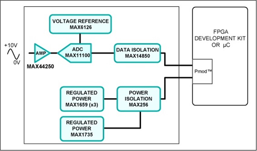
当今许多现场可编程门阵列(FPGA)和微控制器都集成了低分辨率和低输入电压模数转换器(ADC)。然而,它们无法满足需要更高分辨率和更高输入电压的工业控制和工业自动化应用的需求。Fresno (MAXREFDES11)子系统参考设计是一款16位高精度工业模拟前端(AFE),可支持0至10V信号并将隔离电源和数据功能全部集成在一个小尺寸中。Fresno设计集成了超精密低噪声缓冲器(MAX44250);高精度ADC (MAX11100);超高精度4.096V基准电压源(MAX6126);600VRMS数据隔离(MAX14850);以及+5.5V、+5V和-3V隔离/稳压电源轨(MAX256/MAX1659/MAX1735)。该AFE解决方案可用于任何需要高精度模数转换的应用,但主要面向工业传感器、工业自动化、过程控制、可编程逻辑控制器(PLC)和医疗应用。

图1.Fresno子系统设计框图。
优势和特点
特征
- 高精度
- 0至10V输入范围
- 隔离电源和数据
- 印刷电路板(PCB)面积小
- 设备驱动
- C源代码示例
- 兼容Pmod™的外形尺寸
详情


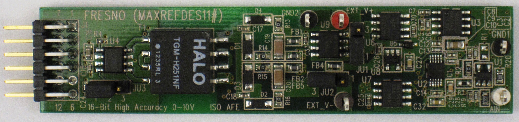
The Pmod specification allows for both 3.3V and 5V modules as well as various pin assignments. This module is designed only for a supply voltage of 3.3V and uses the SPI pin assignments as illustrated on the right.
The power requirements are shown in Table 1. The currently supported platforms and ports are shown in Table 2.
| Power Type | Input Voltage (V) | Input Current (mA, typ) | |
| On-board isolated power | JU1: 1–2 JU2: 2–3 JU3: 1–2 |
3.3 | 71 |
| External power | JU1: 2–3 JU2: 1–2 JU3: 2–3 |
6 | 10 |
| -5 | 2 |
| Supported Platforms | Port |
| Nexys™ 3 platform (Spartan®-6) | JB1 |
| ZedBoard™ platform (Zynq®-7020) | JA1 |
The Fresno hardware design provides isolated power (MAX256) and isolated data (MAX14850) for a high-accuracy, 0 to 10V signal, analog-to-digital conversion application.
The MAX44250 (U1) op amp input circuit attenuates and buffers a 0 to10V signal to match the input range of the ADC (MAX11100), which is 0 to 4.096V.
The MAX11100 (U2) is a 16-bit, successive-approximation register (SAR) ADC with AutoShutdown™ and fast 1.1µs wake-up features. The ADC's reference input is driven by an ultra-high-precision 4.096V voltage reference, the MAX6126 (U3), with 0.02% initial accuracy and a 3ppm/°C maximum temperature coefficient (tempco).
The MAX256 (U4) provides an isolated, functional insulation class power solution that accepts 3.3V and converts it to ±6V using an off-the-shelf TGN-H251NF Halo® transformer with a 1:1 primary to secondary turns ratio plus an external on-board voltage-doubler circuit. Post-regulation is accomplished using the MAX1659 low dropout (LDO) regulator (for +5V) and the MAX1735 low dropout (LDO) regulator (for -3V). Data isolation is accomplished using the MAX14850 (U5) digital data isolator. The combined power and data isolation achieved is 600VRMS.
The signal input impedance of the Fresno subsystem is 5kΩ (R19 + R20). Ideally, the input impedance should be high, but larger resistors induce higher thermal noise and degrade the noise performance. Therefore, the values of the input resistors R19 and R20 are application dependent. Note that when choosing different values for the input resistors to properly attenuate a 10V signal to a 4V signal, R19 = 1.5 × R20.
To use the on-board isolated power supplies, move the shunts on jumper JU1 and JU3 to the 1–2 position and move the shunt on jumper JU2 to the 2–3 position. To use an external power supply, move the shunts on jumper JU1 and JU3 to the 2–3 position and move the shunt on jumper JU2 to the 1–2 position. Connect the ground terminal of the external power supply to the GND2 connector, the +6V to +12V supply to the EXT_V+ connector, and the -3.3V to -5V supply to the EXT_V- connector. See Table 1 for the jumper settings and the input current requirements.
The Fresno firmware design was initially released for the Nexys 3 development kit and targeted a Microblaze™ soft core microcontroller placed inside a Xilinx® Spartan-6 FPGA. Support for additional platforms may be added periodically under Firmware Files in the All Design Files section. The currently supported platforms and ports are shown in Table 2.
The firmware is a working example of how to interface to the hardware, collect samples, and save them to memory. The simple process flow is shown in Figure 2. The firmware is written in C using the Xilinx SDK tool, which is based on the Eclipse™ open source standard. Custom Fresno-specific design functions were created utilizing the standard Xilinx XSpi core version 3.03a. The SPI clock frequency is set to 3.125MHz.

Figure 2. The Fresno firmware flowchart for Nexys 3 platform.
The firmware accepts commands, writes status, and is capable of downloading blocks of sampled data to a standard terminal program via a virtual COM port. The complete source code is provided to speed up customer development. Code documentation can be found in the corresponding firmware platform files.
The Fresno firmware design is also developed and tested for the ZedBoard kit and targets an ARM® Cortex®-A9 processor placed inside a Xilinx Zynq system-on-chip (SoC). An AXI MAX11100 custom IP core is created for this reference design to optimize the sampling rate and the SPI timing stability.
The firmware is a working example of how to interface to the hardware, collect samples, and save them to memory. The simple process flow is shown in Figure 3. The firmware is written in C using the Xilinx SDK tool, which is based on the Eclipse open source standard. Custom Fresno-specific design functions were created utilizing the AXI MAX11100 custom IP core. The SPI clock frequency is set to 4.54MHz when a 189.4ksps sampling rate is selected. The SPI clock frequency is set to 2.5MHz for all other sampling rates.

Figure 3. The Fresno firmware flowchart for ZedBoard platform.
The firmware accepts commands, writes statuses, and is capable of downloading blocks of sampled data to a standard terminal program via a virtual COM port. The complete source code is provided to speed up customer development. Code documentation can be found with the corresponding firmware platform files.
Required Equipment
- Windows® PC with two USB ports
- Fresno (MAXREFDES11#) Board
- Fresno-supported Platform (i.e., Nexys 3 development kit or ZedBoard kit)
- Industrial sensor or signal source
Download, read, and carefully follow each step in the appropriate Fresno Quick Start Guide:
Fresno (MAXREFDES11#) Nexys 3 Quick Start Guide
Fresno (MAXREFDES11#) ZedBoard Quick Start Guide
Equipment Used
- Audio Precision® SYS-2722 signal source or equivalent
- Voltage calibrator DVC-8500
- Windows PC with two USB ports
- Fresno (MAXREFDES11#) board
- Nexys 3 development kit
- +10V power supply
- -5V power supply
Special care must be taken and the proper equipment must be used when testing the Fresno design. The key to testing any high-accuracy design is to use sources and measurement equipment that are of higher accuracy than the design under test. A low distortion signal source is absolutely required in order to duplicate the presented results. The input signal was generated using the Audio Precision SYS-2722. The FFTs were created using the FFT control in SignalLab from Mitov Software.
AC and DC performance for on-board isolated power is shown in Figure 4 and Figure 5. AC and DC performance for external power is shown in Figure 6 and Figure 7.

Figure 4. AC FFT using on-board isolated power, a 0 to 10V 1kHz sine wave input signal, high-impedance input, a 20ksps sample rate, and a Blackman-Harris window.

Figure 5. DC histogram using on-board isolated power; a 5V input signal; a 20ksps sample rate; 65,536 samples; a code spread of 8 LSBs with 96.3% of the codes falling within the three center LSBs; and a standard deviation of 0.785.

Figure 6. AC FFT using external power, a 0 to 10V 1kHz sine wave input signal, a 20ksps sample rate, and a Blackman-Harris window.

Figure 7. DC histogram using external power; a 5V input signal; a 20ksps sample rate; 65,536 samples; a code spread of 7 LSBs with 98.5% of the codes falling within the three center LSBs; and a standard deviation of 0.651.
ARM is a registered trademark and registered service mark of ARM Limited.
Audio Precision is a registered trademark of Audio Precision, Inc.
AutoShutdown is a trademark of Maxim Integrated Products, Inc.
Cortex is a registered trademark of ARM Limited.
Eclipse is a trademark of Eclipse Foundation, Inc.
Halo is a registered trademark of Halo Electronics, Inc.
MicroBlaze is a trademark of Xilinx, Inc.
Nexys is a trademark of Digilent Inc.
Pmod is a trademark of Digilent Inc.
Spartan is a registered trademark of Xilinx, Inc.
Windows is a registered trademark and registered service mark of Microsoft Corporation.
Xilinx is a registered trademark and registered service mark of Xilinx, Inc.
ZedBoard is a trademark of ZedBoard.org.
Zynq is a registered trademark of Xilinx, Inc.
文件和资源
-
MAXREFDES11 Design Files2021/3/10ZIP43 M
-
Solutions For Rapid Prototyping: Answering the Needs of Practicing Engineers2023/8/23PDF784 K
支持与培训
搜索我们的知识库,获取技术问题答案。我们专门的应用工程师团队也会随时为您解答技术问题。