CN0608


概览
设计资源
器件驱动器
软件(如C代码和/或FPGA代码等)用于与元件的数字接口通信。
优势和特点
- Full featured evaluation board for the AD4170-4
- On-board 2.5 V ADR4525 and LTC6655 references
- SMB connectors for AC/DC inputs
- ADXL10002 on-board vibration sensor
- PC control in conjunction with Analog Devices, Inc., SDP (EVALSDP-CK1Z)
- PC software for control and data analysis (time domain and frequency domain)
- Compatible interface with ACE, IIO Scope, Python, and MATLAB
电路功能与优势
This reference design implements a precision weigh scale measurement system using the AD4170-4 and a 6-wire load cell with a sensitivity of 2mV/V and a nominal resistance of 350Ω. The circuit is intended for industrial weighing and process control applications that require accurate measurement of low level load cell signals.
The AD4170-4 enables direct interfacing of the load cell by integrating many of the signal-conditioning and measurement functions required in a weigh scale system. This level of integration reduces component count, simplifies system design, shortens development time, and enables a compact measurement solution.
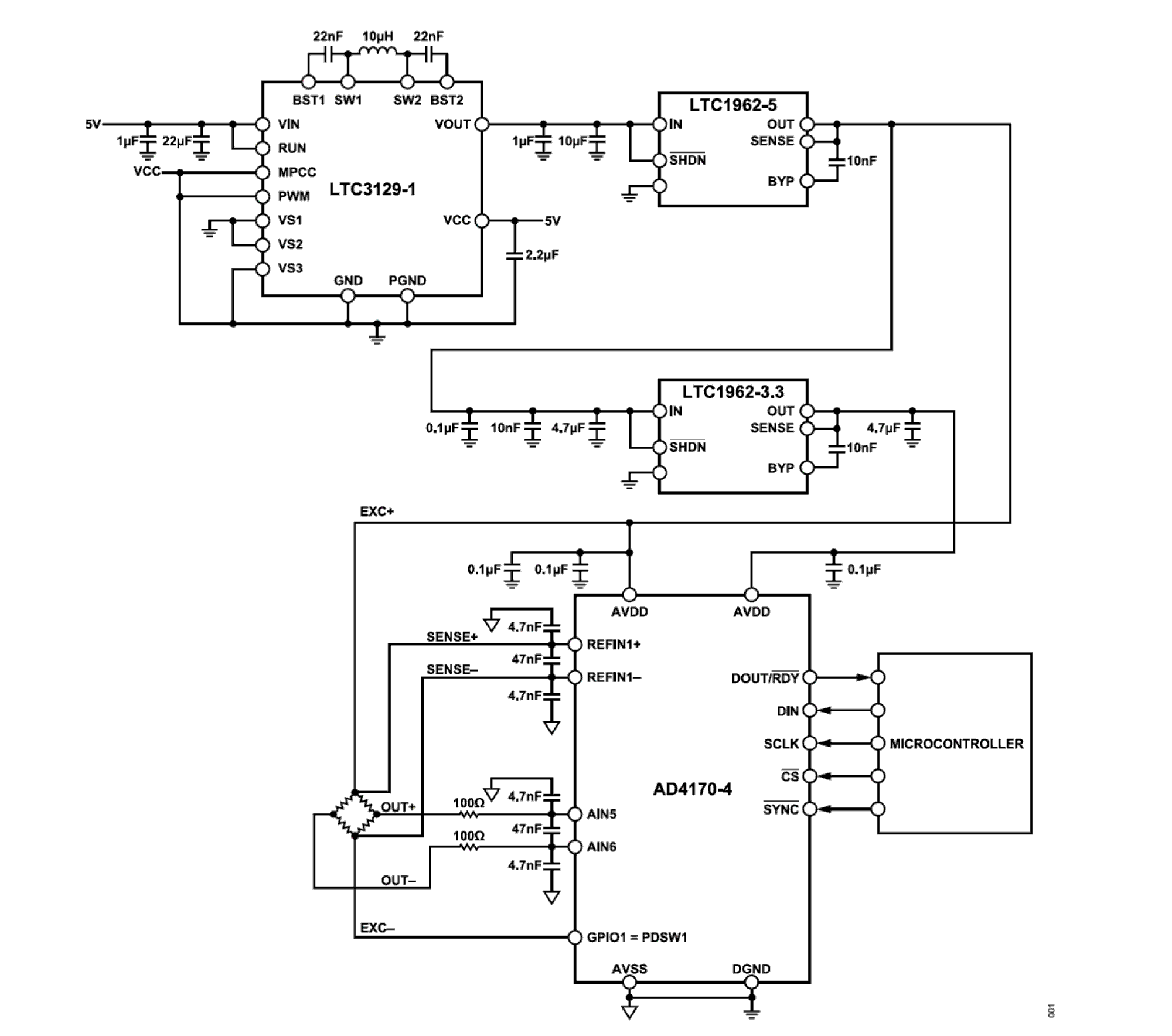
Combined with the load cell interface and filtering network shown in Figure 1, the reference design provides a complete weigh scale solution capable of high resolution weight measurements while minimizing the need for external analog circuitry. The integrated diagnostics also improve system robustness by supporting fault detection and signal chain monitoring.
For the configuration described in this circuit note, the measured system performance achieves a resolution of 32.6mg and 15.9 bits, when operating with the sinc3 filter at an output data rate of 7.63SPS.

电路描述
LOAD CELL INTRODUCTION
A load cell is a sensor that converts an applied force or weight into an electrical signal. Most load cells use strain gauges arranged in a Wheatstone bridge configuration to generate a differential output voltage proportional to the applied load. Load cells are commonly used in industrial weighing systems and process control applications.
Typical load cells have a sensitivity ranging from 0.5mV/V to 2mV/V and a nominal bridge resistance between 180Ω and 1000Ω. For this circuit note, a load cell with a sensitivity of 2mV/V and a nominal resistance of 350Ω is used. The resulting sensor output is typically only a few millivolts and therefore requires amplification before digitization.
Load cells are commonly available in 4-wire and 6-wire configurations. A 4-wire connection consists of excitation and output connections only and is typically used when cable lengths are short. A 6-wire connection adds dedicated SENSE± connections that monitor the excitation voltage directly at the load cell terminals, providing improved measurement performance in applications where cable resistance may be significant.
LOAD CELL MEASUREMENT
To perform a load cell measurement, an excitation voltage is applied across the bridge. The resulting differential output voltage is proportional to the applied load and is measured by the AD4170-4 using a fully differential analog input channel. Because the load cell output is typically only a few millivolts, the integrated PGA is used to amplify the signal before conversion by the 24-bit Σ-Δ analog-to-digital converter (ADC).
Load cell measurements are commonly implemented using a ratiometric configuration. In this approach, the same excitation voltage used to excite the load cell is used as the ADC reference. Because both the load cell output voltage and ADC reference scale proportionally with excitation voltage, variations in the excitation supply are largely cancelled from the measurement result.
To convert the measured ADC output code into weight in grams, a system zero-scale and full-scale calibration must be performed. In load cell applications, the overall measurement accuracy is influenced not only by the ADC but also by the load cell itself, including sensor offset and sensitivity variation. Therefore, system calibration is required to compensate for errors introduced by the complete measurement signal chain.
The AD4170-4 supports system offset and system full-scale calibrations. However, the ADC requires the applied full-scale signal to be at least 80% of the selected ADC full-scale range to perform a system full-scale calibration. Since the output signal from a typical load cell is only a few millivolts, even after amplification by the PGA it does not meet this requirement. Therefore, in this circuit note, both system zero-scale and system full-scale calibrations are implemented in the microcontroller.
System calibration is performed using zero-scale and full-scale calibration. The ADC conversion result acquired with no load applied is stored as the zero-scale (ZS) calibration code, while the conversion result acquired with a known calibration weight is stored as the full-scale calibration code (FS CODE).
The applied weight is calculated using Equation 1:

where:
LOAD is the applied weight in grams.
CODE is the ADC output code.
FS WEIGHT is the applied full-scale weight in grams.
FS CODE is the full-scale calibrated code.
ZS CODE is the zero-scale calibrated code.
CODE is the signed ADC output code.
As an example, the code read from the AD4170-4 when configured in unipolar mode, and with an applied load of 1000 grams is equivalent to 2246784 decimal. The calibrated zero-scale code is 173182 decimal, while the calibrated full-scale code for a full scale weight of 2000g is 4320386 decimal.
The applied weight is calculated using Equation 1.
CODE = 0x224880 or 2246784 in decimal
FS WEIGHT = 2000g
FS CODE = 0x41EC82 or 4320386 in decimal
ZS CODE = 0x02A47E or 173182 in decimal


LOAD CELL DESIGN CONSIDERATIONS
The following sections discuss the key design considerations for the load cell measurement circuit shown in Figure 1. Key design considerations including power supplies, gain selection, reference configuration, filtering, calibration, and load cell interface options are discussed to help optimize system performance and accuracy.
The Load Cell Configuration section describes the available load cell wiring techniques and their implementation. All design considerations and calculations are available in this section.
ADC
In addition to the load cell characteristics, the overall accuracy and resolution of the weigh scale system are heavily influenced by the performance of the ADC. The AD4170-4 provides an integrated solution for precision load cell measurements by combining a 24-bit Σ-Δ ADC, low noise programmable gain amplifier (PGA), and integrated reference buffers in a single device.
The AD4170-4 offers high resolution, low nonlinearity, and low noise performance, and simultaneous 50Hz and 60Hz rejection, making it well suited for industrial weigh scale applications where small sensor signals must be measured accurately in the presence of line frequency interference. The integrated diagnostic features further enhance system robustness by providing analog input monitoring, reference and supply checks, signal chain diagnostics, and serial peripheral interface (SPI) cyclic redundancy check (CRC) protection. These capabilities allow potential faults to be detected without requiring extensive external monitoring circuitry, simplifying system design while improving reliability and diagnostic coverage.
Power Supplies
The AD4170-4 includes separate analog and digital power supplies. Isolating the analog and digital supplies helps minimize the coupling of digital switching noise into the precision analog signal path and preserves measurement accuracy. The device supports an independent digital interface supply (IOVDD) from 1.7V to 5.25V referenced to DGND, allowing direct interfacing to a wide range of host processors and logic levels.
The circuit shown in Figure 1 operates from a single 5V system supply that is also used by the microcontroller. Since a single supply is used, AVSS and DGND are tied together, allowing a common ground plane to be used. Separated low noise supplies are generated from this system supply using low-dropout regulators (LDOs) for AVDD and IOVDD to reduce noise coupling.
To ensure a low noise supply for both the AD4170-4 and the load cell excitation circuitry, low noise linear regulators are used. The LT1962-5 generates the 5V analog supply for AVDD, while the LT1962-3.3 generates the 3.3V IOVDD.
Analog Inputs and Gain Selection
Load cell sensors typically produce very small differential output signals and therefore require amplification before being digitized by the ADC. For this reference design, a load cell with a sensitivity of 2mV/V and a 5V excitation voltage is used, resulting in a maximum differential output signal of:

The AD4170-4 includes an integrated low noise PGA with selectable gains from 1 to 128, allowing direct interface of low-level bridge signals without the need for an external amplification stage. The PGA presents a high input impedance to the load cell and has a typical input current of 25nA at a gain of 128, minimizing sensor loading and preserving measurement accuracy.
To maximize utilization of the ADC input range and achieve the highest possible measurement resolution, the PGA gain is configured to 128. With this gain setting, the maximum 10mV full-scale load cell output is amplified to 1.28V differential.
This amplified signal remains within the allowable input range of the AD4170-4 while making more effective use of the ADC input range. As a result, the system can accurately measure the small output variations generated by the load cell, improving the overall measurement resolution of the weigh scale.
Reference and Reference Buffer
For the circuit shown in Figure 1, the ADC reference inputs are connected to REFIN1+ and REFIN1-. The same 5V excitation source used to power the load cell is also used as the ADC reference. In a 6-wire load cell configuration, the SENSE± wires are connected to the reference inputs, allowing the ADC to measure the actual excitation voltage present across the bridge.
The AD4170-4 reference inputs are continuously sampled by an internal switched capacitor. As a result, large resistor-capacitor (RC) filter values on the reference input can introduce gain errors into the measurement. To avoid this, the internal reference buffers are enabled. The reference buffers isolate the switched capacitor sampling from the external circuitry, allowing the use of higher resistor values and electromagnetic compatibility (EMC) filtering components without degrading measurement accuracy.
The AD4170-4 includes rail to rail reference buffers, allowing the full reference voltage range to be utilized without requiring additional voltage headroom. This simplifies the interface between the load cell and the ADC while maintaining accurate operation across the supported reference voltage range.
Power Down Switch
Load cells can consume a significant amount of current due to their relatively low bridge resistance. For example, a 350Ω load cell excited with a 5V supply draws approximately 14.3mA.
In applications where continuous measurements are not required, disconnecting the load cell between measurement cycles can significantly reduce overall system power consumption. To support this functionality, the AD4170-4 includes two integrated bridge power-down switches, PDSW0 and PDSW1, which are used to disconnect the load cell excitation path when the bridge is not in use. Each switch can withstand up to 30mA of continuous current and has an on resistance of 14Ω maximum.
For this reference design, PDSW1 is used to control the load cell excitation path. Although the switch on resistance introduces a small voltage drop, this does not impact measurement accuracy because the load cell output signal and ADC voltage reference are derived from the same excitation source.
Digital and Analog Filtering
External RC filtering is required on the analog inputs and reference inputs of the AD4170-4. These RC networks serve as anti-alias filters to reject any interference at the modulator frequency and any multiples of this frequency.
The AD4170-4 has several digital filter options that provide selectable tradeoffs between output data rate, settling time, noise performance, and simultaneous 50Hz and 60Hz rejection. Unlike the external RC filters, which primarily attenuate out of band signals that could alias into the measurement, the selected digital filter directly impacts the achievable noise free resolution and digital filter settling time.
For this circuit note, the sinc3 filter is selected because it provides excellent noise performance for single-channel load cell measurements operating at low output data rates, making it well suited for precision weigh scale applications.
Calibration
The AD4170-4 supports both internal and system calibration modes. For this reference design, system calibration is implemented in the microcontroller to compensate for errors introduced by the overall measurement chain, including the load cell and signal conditioning circuitry. The AD4170-4 analysis, control, evaluation (ACE) plugin includes a demo mode that simplifies the calibration process and generation of the calibration coefficients used for weight measurements.
LOAD CELL CONFIGURATION
Load cells are 4-wire or 6-wire. Both types use a differential bridge output voltage to measure the applied load. However, they differ in how the excitation voltage is sensed at the load cell. The choice of 4-wire versus 6-wire impacts the overall measurement accuracy, particularly in applications with long cable lengths or low-level sensor signals.
For this circuit note, a 6-wire load cell with a sensitivity of 2mV/V is used. This approach provides the highest measurement accuracy by allowing the excitation voltage at the load cell terminals to be sensed directly and used as the ADC reference. The following sections describe the implementation of both connections and their associated design considerations.
4-Wire Bridge
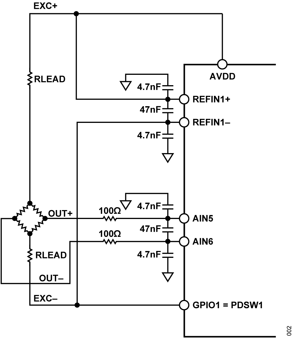
With a 4-wire bridge, the excitation is applied directly to the bridge, while the ADC measures the differential voltage developed across the load cell output terminals. When the excitation voltage is not sensed at the load cell, any voltage drop across the excitation leads reduces the actual bridge excitation voltage seen by the sensor. Since the load cell output is proportional to excitation voltage, this reduction introduces a gain error that increases with lead wire resistance and cable length.
Figure 2 shows the 4-wire bridge interfaced to the AD4170-4. The bridge output is connected to the ADC analog inputs while the excitation voltage is used as the ADC voltage reference. Although this simplifies wiring connectivity, the measurement accuracy can be affected by excitation lead resistance, particularly in remote sensing applications or installations with long cable runs.

6-Wire Bridge
Figure 3 shows the connection of a 6-wire load cell to the AD4170-4. The load cell differential output is connected to AIN5 and AIN6, which are configured as a fully differential input channel. The voltage excitation used to excite the load cell is generated by the LT1962-5 and provides the 5V supply for the AVDD. The SENSE+ and SENSE− wires are connected to REFIN1+ and REFIN1−, respectively, providing the ADC reference voltage. The PDSW1 pin is connected to the negative excitation terminal and is used to control the bridge excitation path.

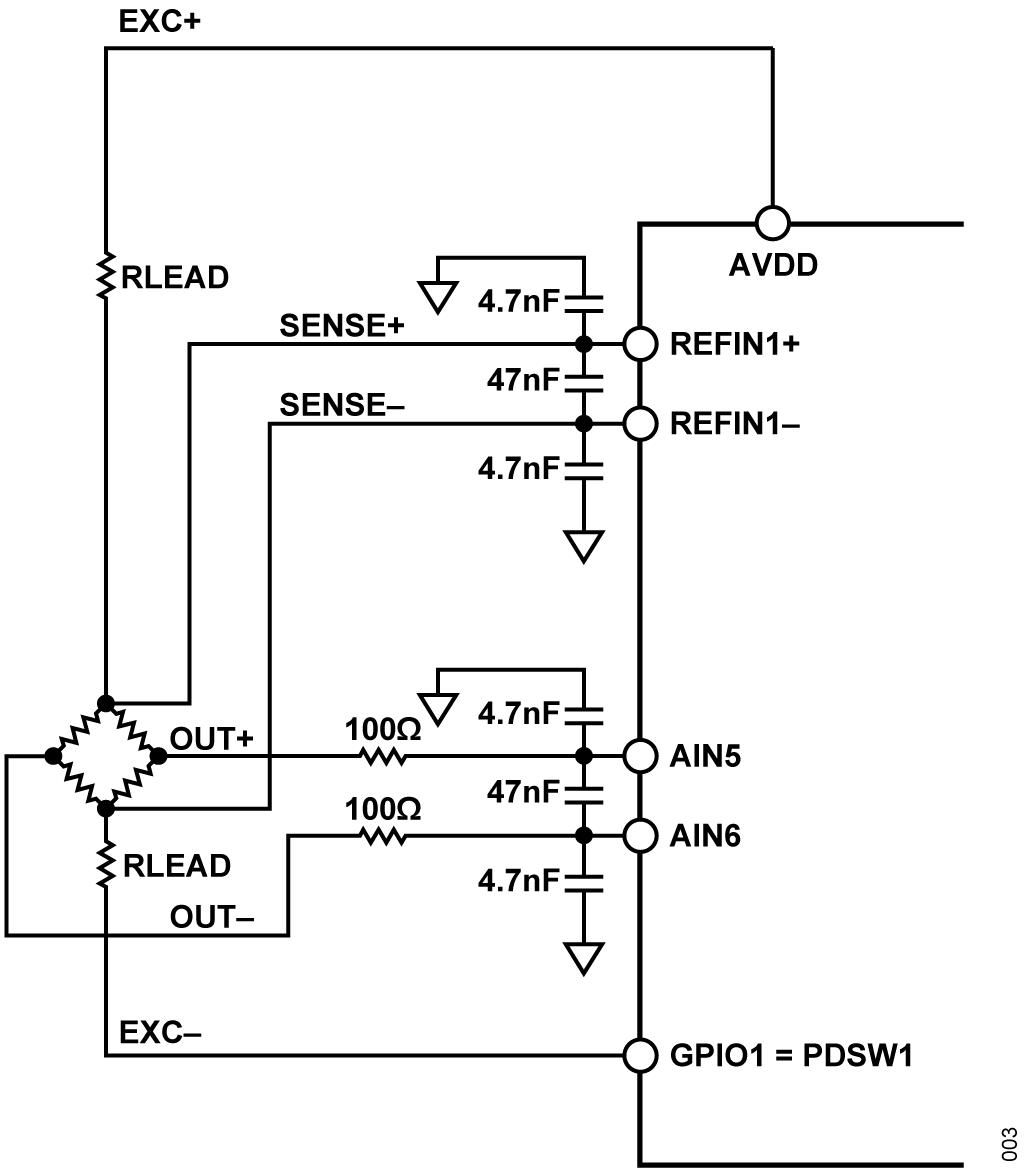
The external RC filter networks connected to the analog and reference inputs provide anti-alias filtering. The AD4170-4 configuration used for the 6-wire bridge measurement is shown in Table 1.
| Parameter | Setting |
| Differential Input | AIN+ = AIN5 AIN− = AIN6 |
| Excitation Voltage | 5V |
| Gain | 128V |
| Reference Buffers | Enabled |
| Power Down Switch | PDSW1 Enabled |
| Digital Filter | Sinc3, 7.63SPS |
| Applied Load | 1kg |
The selection of the gain, reference configuration, and digital filter settings is based on the design considerations described in the Load Cell Design Considerations section. This configuration maximizes measurement resolution while maintaining excellent noise performance for precision weigh scale applications.
6-Wire Bridge Results
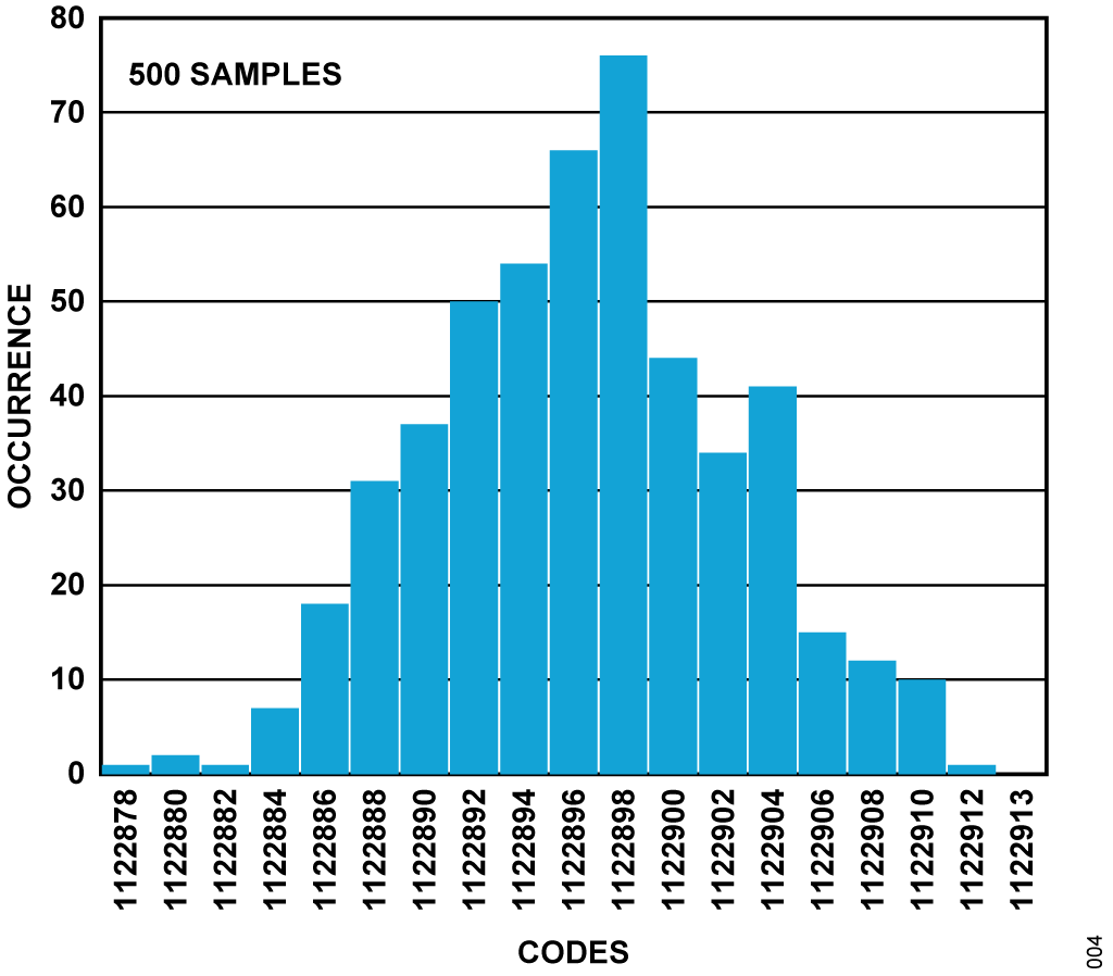
For the load cell circuit shown in Figure 3, data was gathered using the sinc3 digital filter with an output data rate of 7.63SPS. A total of 500 conversions were recorded with a 1kg load applied to the load cell.
Figure 4 shows the resulting noise distribution of the ADC conversion results with a 1kg load applied to the load cell. From the 500 samples collected, the peak-to-peak noise of the system was 162.995nV. This measured noise level is used to determine the achievable noise free counts, resolution in weights, and noise free resolution of the system.

For a load cell with a full scale output of 10mV, the corresponding number of noise free counts is calculated as:

Using a full scale measurement range of 2kg, the achievable weight resolution is:

The corresponding noise free resolution is:

The measured performance corresponds to 61,352 noise free counts, 32.6mg weight resolution, and 15.9 bits of noise free resolution.
常见变化
In addition to voltage excitation, current excitation can also be used. When implementing a current excited load cell measurement, a ratiometric configuration is still required to maintain measurement accuracy. Current excitation forces the same excitation current to flow through the bridge, making the measurement less sensitive to lead wire resistance while causing the load cell output voltage to vary directly with the bridge resistance.
The AD4170-4 includes programmable excitation current sources that can be routed to either the analog inputs or GPIO pins. When using these current sources, the output compliance voltage must be considered because sufficient voltage headroom is required to maintain the programmed excitation current. The compliance voltage therefore places an upper limit on the allowable load cell voltage.
电路评估与测试
EQUIPMENT NEEDED
The following equipment is required for the load cell measurement system:
- The EVAL-AD4170-4ARDZ evaluation board
- The EVAL-SDP-CK1Z system demonstration platform (SDP)
- The ACE software
- A power supply that is USB powered
- A load cell
- A PC running Windows® with a USB 2.0 port
SOFTWARE INSTALLATION
A complete software user guide for the AD4170-4 and the EVALSDP- CK1Z can be found in the EVAL-AD4170-4ARDZ user guide and the SDP User Guide.
The ACE software is required to interface with the hardware. Download the ACE software and then follow the installation setup from the installing the ACE software section of the EVAL AD4170-4 user guide. Install the evaluation software before connecting the EVAL-AD4170-4ARDZ and the EVAL-SDP-CK1Z to the USB port of the PC to ensure that the evaluation system is recognized correctly when connected. After the evaluation software installation is complete, connect the EVAL-SDP-CK1Z to the EVAL-AD4170-4ARDZ and then connect the EVAL-SDP-CK1Z to the USB port of the PC using the supplied cable. Launch the ACE software, download, and install the AD4170-4 ACE plugin. Refer to the EVALAD4170- 4ARDZ user guide for the complete installation guide of the AD4170-4 ACE plugin.
SETUP AND TEST
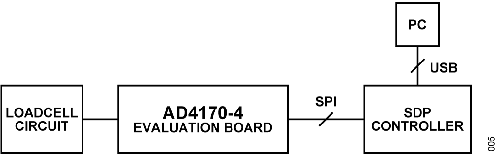
Do not connect the power to the hardware until both the EVALAD4170- 4ARDZ and the EVAL-SDP-CK1Z are connected, and the links are properly configured for a load cell application. Figure 5 shows a functional block diagram of the test setup for a 6-wire bridge.

The EVAL-AD4170-4ARDZ is required to test the circuit. In addition, a 6-wire, 350Ω load cell with a sensitivity of 2mV/V must be used. To achieve performance comparable to the results presented in this circuit note, modify the on-board analog input and reference input RC filter components on the EVAL-AD4170-4-ARDZ to the values shown in Figure 1.
To configure the hardware, configure the system as follows:
- Set all links on the EVAL-AD4170-4ARDZ for load cell configuration
as shown in Figure 6.

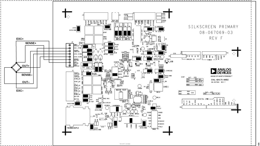
Figure 6. EVAL-AD4170-4ARDZ Load Cell Hardware Link Configuration - Connect the EVAL-SDP-CK1Z to the EVAL-AD4170-4ARDZ evaluation board via the Arduino headers.
- Connect the load cell in 6-wire bridge configuration.
- Connect the EVAL-SDP-CK1Z to the PC via the USB cable.
- Run the ACE software.
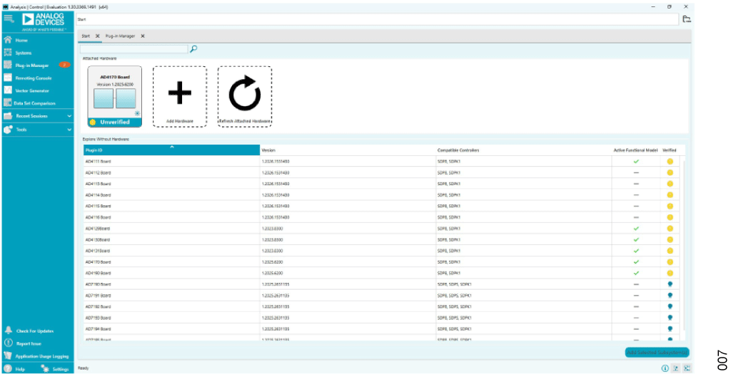
- The ACE software must be able to detect the EVALAD4170- 4ARDZ board as shown in Figure 7.
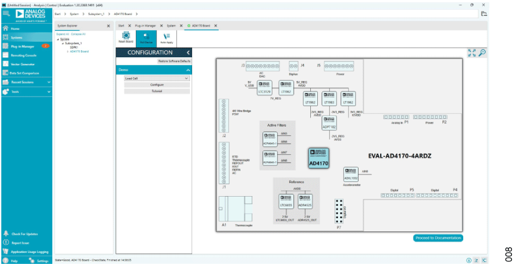
- Double click the AD4170 Board icon to open the AD4170 board view as shown in Figure 8, and select the load cell demo mode.
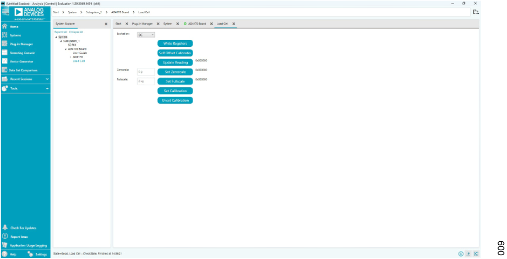
- Set the necessary values in the Load Cell demo mode, click on the Write Registers icon, then apply the zero load and full-scale load, and perform the calibrations.
- For more details about the ADC register map settings, calibration, and measurement procedures, refer to the tutorial section of the AD4170 plugin.