概览
设计资源
评估硬件
产品型号带"Z"表示符合RoHS标准。评估此电路需要下列选中的电路板
- EVAL-CN0586-ARDZ ($179.11) Circuit Evaluation Board
- EVAL-SDP-CK1Z ($184.00) System Demonstration Platform
参考资料
-
EVAL-CN0586-ARDZ User Guide2024/7/22WIKI
-
CN0586: Precision High Voltage Bipolar Analog Output Module (Rev. 0)2024/7/8PDF746 K
电路功能与优势
With the continued advancement of electronic systems, the field of electronic test and measurement continues to demand faster, more precise, and robust testing capabilities. In this landscape, precision high-voltage solutions play a key role in providing accurate stimulus for evaluating the next generation commercial, industrial, or automotive applications, liquid-crystal display (LCD) and organic light-emitting diode (OLED) panels testing for smart devices, biasing standard silicon photodiodes (SiPDs) or avalanche photodiodes (APDs) for light detection and ranging (LiDAR) in both automotive and industrial applications, piezoelectric positioning and actuation, microelectromechanical systems (MEMs) mirror control, and more.
Analog Devices provides a variety of solutions and products centered around high-voltage applications and this reference design is just a drop in the bucket!
The circuit shown in Figure 1 is a precision bipolar high voltage drive solution, with up to 200 V output span, and digital interface isolation. This solution utilizes a 4-channel, 16-bit precision digitalto-analog converter (DAC) and a 220 V precision amplifier in a configuration capable of providing bipolar output ranges from a unipolar source. An on-board power solution is also included to provide +110 V and −110V from a single 15 V input supply to aid in quick evaluation of this reference design. Providing all the signal chain components into the evaluation board significantly eases the design of high voltage output drive systems.
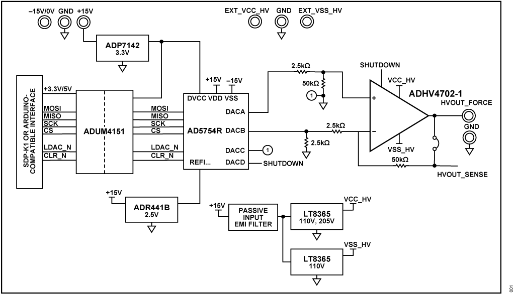
Figure 1. Circuit Diagram.
The evaluation hardware is partnered with the SDP-K1, which enables easy integration with other Arduino-UNO-based controller boards. The software interface is available in analysis, control, and evaluation (ACE) software as a plug-in, providing easy installation and usage. The plug-in communicates with the control board through an open-source firmware loaded in the SDP-K1, allowing for quick adaption to user-end systems and platforms.
电路描述
The CN0586 features a high voltage driver signal chain through the combination of a precision DAC and a high voltage precision operational amplifier. This reference design provides high voltage output ranges of up to 200 V and with the on-board power solution, the EVAL-CN0586ARDZ can provide +/−100 V output from a 15 V external supply.
Figure 1 shows the connection of the AD5754R's two DAC output channels (A and B) to the high voltage amplifier, ADHV4702-1, configured with external resistors to provide a gain of 20. The output transfer function of this circuit is given by the equation:

where:
DA is the decimal code loaded to DAC Channel A (Main DAC).
DB is the decimal code loaded to DAC Channel B (Offset DAC).
Gain is the scaling factor for the different output voltage range of the DACs. "2" for +5 V, "4" for +10 V.
VREF is the voltage reference with a nominal value of 2.5 V.
20 is the HV amplifier stage gain.
The Main DAC output range setting determines the end-to-end output span of the circuit while the Offset DAC value determines the center point of the total output range. With the configuration of external gain settings resistors on the ADHV4702-1, the circuit is Table 1. HV Output Ranges able to provide high voltage outputs ranges up to 200 V and drive capability of up to 20 mA.
The high voltage output range, and upper and lower limits can be calculated using the following formulas:
HVOUTSPAN = |VMAINFS - VMAINZS| × 20
HVOUTUPPER = (VMAINFS - VOFFSET) × 20
HVOUTLOWER = (VMAINZS - VOFFSET) × 20
where:
VMAINFS is the voltage output of the main DAC with Full-scale code loaded.
VMAINZS is the voltage output of the main DAC with Zero-scale code loaded.
VMAINFS is the voltage output of the main DAC with Full-scale code loaded.
VOFFSET is the voltage output of the offset DAC.
The high voltage output ranges shown in Table 1 are combinations of AD5754R's Main DAC and Offset DAC configurations, and supported by the EVAL-CN0586-ARDZ with its on-board switching-mode power supplies.
| Main DAC | Offset DAC | HV Output Range | Output Span |
| 0 V to 10 V | 0 V | 0 V to +200 V | 200 V |
| 0 V to 10 V | 5 V | −100 V to +100 V | 200 V |
| 0 V to 5 V | 0 V | 0 V to +100 V | 100 V |
| 0 V to 5 V | 2.5 V | −50 V to +50 V | 100 V |
If both the Main DAC and Offset DAC are set to the +10 V range, the EVAL-CN0586-ARDZ can support all the HV output range configurations outlined in Table 1.
LTSpice Simulation
The reference design can be quickly simulated in LTSpice using the circuit in Figure 2. In this case, the high voltage amplifier circuitry is simulated while replacing DAC channel outputs with ideal voltage sources. The V1 source acts as DAC A or the Main DAC while the V2 source acts as DAC B or the Offset DAC.
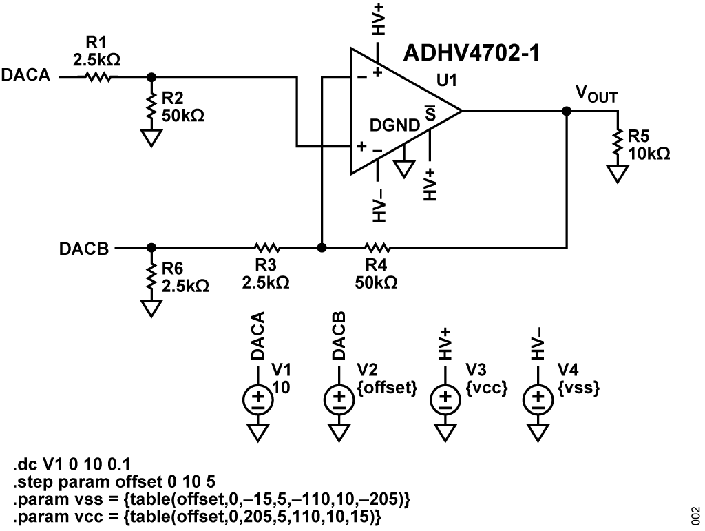
Figure 2. LTSpice® Circuit.
The set of spice directives set a DC sweep of V1 (Main DAC) across its 10 V range equating to a span of 200 V. Meanwhile, this simulation is run on different DC values of V2 (Offset DAC), resulting in multiple 200 V span plots across different offset levels, as shown in Figure 3.

Figure 3. Output Span Simulation.
Simulation files are available on the design resources page.
DAC Features
The core part of the design is the AD5754R, a quad, 16-bit, serial input, voltage output digital-to-analog converter (DAC). The DAC contains an on-chip 5 ppm/°C 2.5 V reference and has software selectable output ranges of +5 V, +10 V, +10.8 V, +/−5 V, +/−10 V, and +/−10.8 V. For nominal full-scale output range, the DAC is operated with the dual supply voltage of +/−15V. In this application, only the +5 V and +10 V output ranges are used.
The AD5754R is controlled using a serial interface compatible with serial peripheral interface (SPI), digital signal processing (DSP), and microcontroller interface standards, and runs at a maximum of 30 MHz clock. The DAC has an I/O pin, BIN/2SCOMP, to select the input code format for writing to the DAC registers. For the firmware used in this reference design, binary coding is chosen.
A feature of the DAC utilized in this design is the asynchronous CLR, which makes use of the active low/CLR pin to reset the DAC to either the zero-scale or mid-scale code. Activating clear (CLR) sets all the DAC channel outputs to the desired known state useful for system reset.
HV Amplifier
The high voltage driver at the end of the signal chain is the ADHV4702-1. This next generation operational amplifier from Analog Devices offers precision performance with 1 mV input offset, 170 dB open loop gain, and 160 dB common-mode ripple rejection, while operating with +/−110 V asymmetrical dual supplies or up to 220 V single supply and typical output current of 20 mA. The ADHV4702-1 also offers excellent dynamic performance with a small signal bandwidth of 10 MHz and a slew rate of 74 V/µs. It has on-chip safety features such as thermal monitoring and shutdown, essential for high voltage applications.
HV Power Solution
The on-board high voltage power rails are provided by the LT8365 low quiescent current, current mode DC/DC converter with a 1.5 A, 150 V internal switch, operating from a 2.8 V to 60 V input. The LT8365 features a unique single feedback pin architecture, making it capable of boost, single-ended primary-inductor converter (SEPIC), or inverting configurations. In this reference design, two LT8365 circuit are included to provide the different configurations for the positive and negative high voltage output rails.
There are two LT8365 circuitry on board the EVAL-CN0586-ARDZ configured to provide the dual high voltage supplies needed by the high voltage driver. A switch allows to easily change the high voltage supplies outputs, as shown in Table 2. Refer to the schematic for more information.
| S1 | HV VCC | HV VSS |
| Pos A | +205 V | 0 V (disabled) |
| Pos B (default) | +110 V | −110 V |
Important note: Set the HV outputs before power is supplied to the board to avoid potential damage to the user and on-board circuitry.
Custom HV Output Ranges
The EVAL-CN0586-ARDZ offers predetermined HV output ranges, as outlined in Table 2. With the flexibility of the DAC that controls the HV output, it is important to consider optimizing the HV supply for the target range of operation. Circuit Description provides guidance on calculating the output range.
For example, if the target HV output range is −20 V to 80 V with a 10 mA load, then having a +/−100 V supply is not practical. As much as 800 mW of power is just dissipated by the HV driver. In this case, it can be highlighted that the ADHV4702-1 only has a 2 V headroom requirement. This means as low as 2 V headroom on each supply rail is needed for an optimized power solution.
Safety Considerations
Digital Isolation
In high voltage applications, it is important to protect the area of the circuit operating in the low voltage region. In this reference design, a digital isolator protects the controller board, EVAL-SDP-CK1Z, in case of high voltage faults in the driver section. The ADUM4151 is the digital isolator optimized for isolating serial peripheral interfaces (SPI) that can provide SPI clock rates up to 17 MHz with 35 kV/µs transient immunity. The ADUM4151 also provides three additional low data rate isolated channels for independent digital control. The device follows UL, CSA, and VDE standards for safety and regulatory approvals. See the Common Variations section for alternatives to the ADUM4151.
Protecting the AD5754R Output
The HV amplifier, ADHV4702-1, can be configured for a maximum output voltage of 220 V. To protect the output of the AD5754R, a 2.5 kΩ resistor terminated to ground is added to the Offset DAC, Channel B, as shown in Figure 4. This protection resistor, together with the 50 kΩ and 2.5 kΩ gain setting resistors (and the dual supplies of AD5754R), ensures that the absolute maximum ratings of the DAC outputs are never violated.
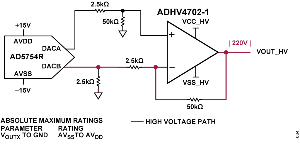
Figure 4. DAC Output Protection Circuit.
With the combination of resistors, a voltage divider is formed, making sure the voltage in the hv feedback loop, as seen in the DAC output, never exceeds |220| x 2.5 / (2.5 k + 2.5 k + 50 k) = |9.1V|, which is within the absolute maximum ratings of the AD5754R (refer to the data sheet for more info). One disadvantage of this configuration is that the output of the DAC consumes power through the 2.5 kΩ protection resistor, causing some self-heating.
The 2.5 kΩ protection resistor does not affect the HV amplifier gain. Smaller values can be used but a certain balance needs to be found between the voltage protection and the current consumption, and the self-heating induced by the resistor.
Software Shutdown
The EVAL-CN0586 has a software-controlled shutdown feature that utilizes a firmware command sequence and the "Asynchronous Clear" function of the AD5754R DAC. As seen from Figure 1, an extra DAC output (Channel D) is connected to the ADHV4702-1 shutdown pin. The firmware command sequence sets the DAC Channel D low, effectively shutting down the output of the HV amplifier. It also sets the outputs of the Main (Channel A) and Offset (Channel B) DACs to the same output voltage value, resulting in a 0 V output.
The /SD pin is pulled down by default and supports 2.5 V logic so the DAC can be replaced by a general-purpose input/output (GPIO).
Overtemperature Shutdown
The system can avoid performance degradation due to operating beyond the maximum temperature specification by leveraging the shutdown and thermal monitoring features of the ADHV4702-1. To implement this, the /SD pin can be tied to the TMP pin using the on-board jumper, JP4, which allows the TMP pin voltage to assert the device shutdown. Refer to the ADHV4702-1 data sheet for more details on this feature.
When overtemperature shutdown is selected using JP4, DAC-controlled (software) shutdown for HV amplifier is disabled. Clear function is not affected.
Power On Reset (POR)
The AD5754R has a POR circuitry that ensures the DAC registers power-up loaded with zero code and all DAC channels are in power down mode. This means all inputs to the HV driver circuit and the HV output are set to 0 V as well.
Slew Rate Protection
With continuous operation at or near full bandwidth of the ADHV4702-1, there is increased supply current that affect the junction temperature, TJ, of the device. In this design, the recommended input clamping method using BAV1999LT1G is adopted. Clamping the differential input voltage in this manner dampens the slew rate and reduces the large signal bandwidth of the ADHV4702-1, but protects it in dynamic operation.
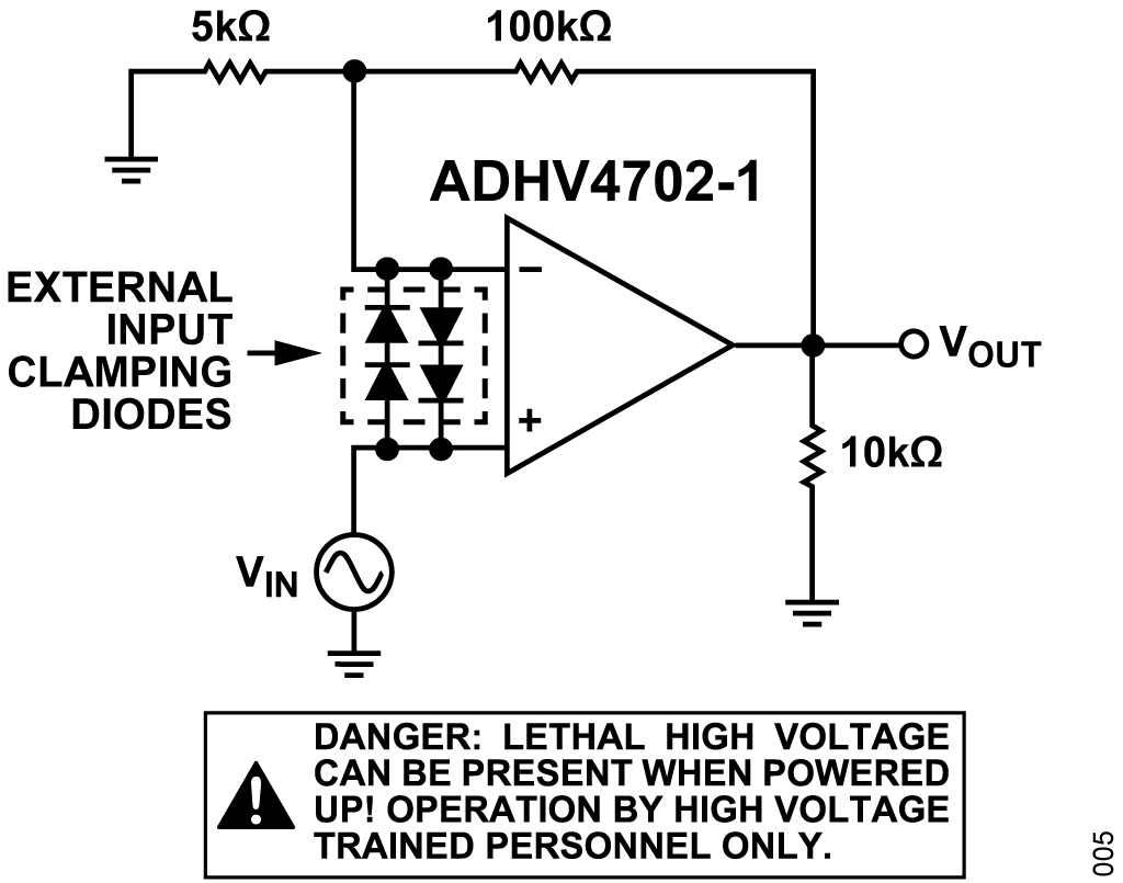
Figure 5. ADHV4702-1 Slew Rate Protection Circuit.
Safe Operating Area (SOA)
It is critical in high voltage applications to understand the SOA of a device as it represents the device's power handling capability. In CN0586, the ADHV4702-1 is in charge of the driving stage and thus its SOA must be carefully reviewed. Operating in high frequencies, for example, increases the current consumption of the device, which directly increases the junction temperature, TJ. See the product data sheet for more info.
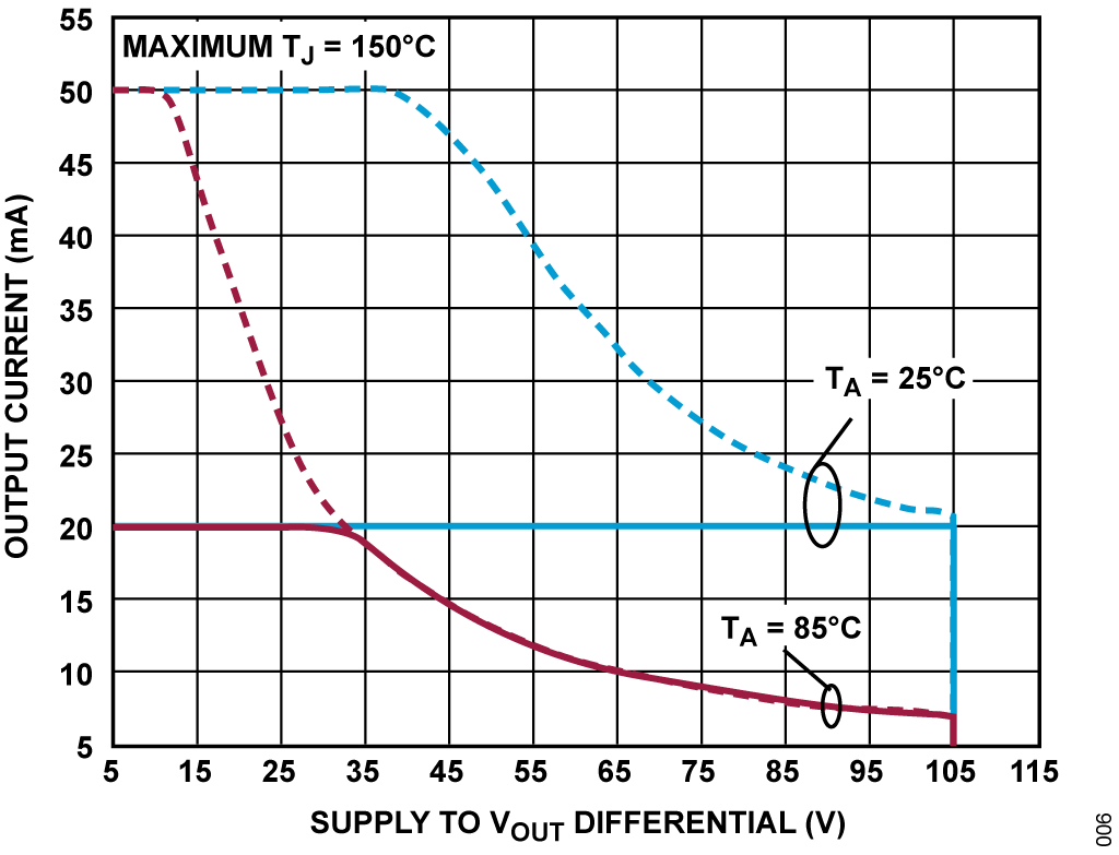
Figure 6. ADHV4702-1 DC SOA.
The plot above depicts the ADHV4702-1’s DC SOA and it shows the curve of output current versus the voltage across the output stage of the op-amp. When operating at DC, the device dissipates the power that comes from the difference of the output voltage and supply, and the current being drawn by the load. The areas under the curve shows the boundaries for safe operation to maintain a TJ ≤ 150 C.
To calculate for the estimated junction temperature, use this formula:
TJ = [(VSYS - VOUT) × ILOAD + (VSYS × ISYS)] × θJA + TA
where:
VSYS is the total supply denoted by |VCC-VSS|
ISYS is the device power consumption.
θ;JA is the junction to ambient thermal resistance of the part.
TA is the ambient temperature the device is operating at.
Both the SOA curve and the θ;JA of a device are parameters unique to the condition under which the product is tested. It is good design practice to have a tolerance when calculating using these parameters.
Grounding and Isolation
As discussed in prior sections, the CN0586 uses a digital isolator to protect the control boards, PC, and other peripherals intended for digital control. These devices are usually terminated to the earth ground. To maintain the designed protection, it is recommended that the external supplies used to power the EVAL-CN0586-ARDZ should be floating or provides some isolation to earth ground.
The PCB is also designed to easily recognize the high voltage area from the digital area, as seen from Figure 7. The HV area is also protected by a polycarbonate cover on top and a conformal coating at the bottom, enhancing user safety.
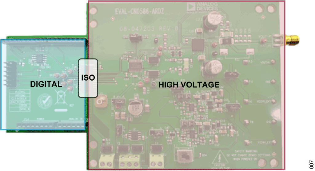
Figure 7. PCB Area Isolation.
常见变化
This section outlines the common variations that can be applied in this reference design.
For the DAC, a minimum of two channels is needed for main and offset control. A smaller DAC solution, the AD5689R, a 16-bit, dual compact voltage output DAC, with internal reference can be considered. It provides the similar accuracy but in a smaller 3 mm × 3 mm footprint.
For higher density systems, the AD5676R, a 16-bit, 8-channel DAC is the better fit. This device also provides an on-board reference and comes in a smaller ~2 mm × 2 mm WLCSP package.
HV driver variations: for higher current drive requirements, the LTC6090, a 140 V rail-to-rail op-amp, can be used as an alternative. Although the maximum voltage range is decreased, it can provide up to 50 mA of drive current to the target load.
For an integrated solution, the AD8460 is capable of delivering 80 V output span, 1 A continuous drive current, 1.8 kV/μs slew rate into a 1000 pF load, and 1 MHz of bandwidth HV driver, co-packaged with a 14-bit high-speed DAC. This “bits in, power out” solution also comes with digital features like built-in arbitrary waveform generator (AWG), digitally programmable current, voltage and thermal fault monitoring, and more! See product data sheet.
The ADHV4702-1 itself can also be modified to provide higher current drive. Figure 8 shows a configuration that increases the current drive capability of any amplifier. Utilizing a discrete unity-gain stage, the original amplifier’s precision performance capabilities are retained while maximizing the current handling specifications of the discrete devices.
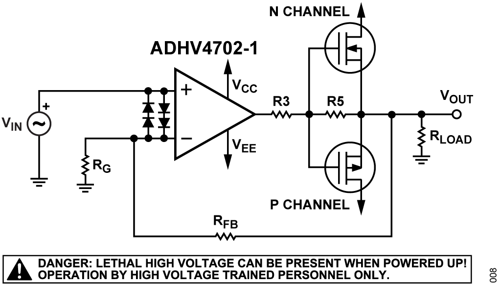
Figure 8. ADHV4702-1 High Current Output Drive Schematic.
In terms of the power solution, the LT8365 offers output voltages of upto +/−420 V with the use of boost and voltage doubler configurations. Figure 9 is taken from one of the typical applications in the product data sheet.
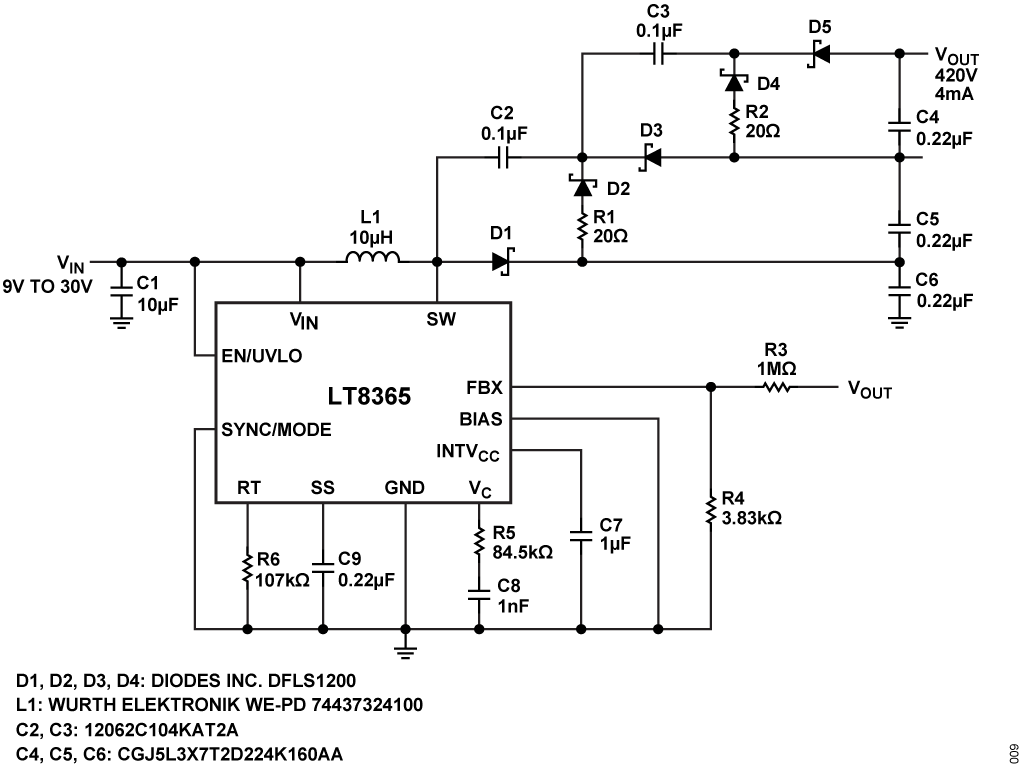
Figure 9. LT8365 420 V Output Configuration.
电路评估与测试
The EVAL-CN0586-ARDZ is paired up with the EVAL-SDP-CK1Z STM32F469NIH6 Arm® Cortex®-M4-based microcontroller board with digital peripherals available on Arduino® Uno-compatible headers. For complete software and hardware setup and other important information, refer to the CN0586 user guide.
Equipment Needed
- EVAL-CN0586-ARDZ
- EVAL-SDP-CK1Z
- +/−15V Power Supply
- PC with Microsoft Windows 10 OS or Higher
Quick Setup and Test
- Make sure the jumpers and switch are set to the default positions, as discussed in the user guide. Connect the evaluation board to the SDP-K1 board.
- Connect the external +/−15V power supplies to P1, as shown in Figure 10. Make sure that the board cover is attached for safety and then turn on the power supplies.

Figure 10. Hardware Setup.
- Once the board is powered on, connect the USB Type C cable between the SDP-K1 board and the PC. To validate successful connection, look for the DS2 LED with label SYS PWR on the SDP-K1 board. If the LED is blinking red, then there might be some issues.
- Run the ACE application. On the "Start" window of ACE, the EVAL-CN0586-ARDZ should appear in the “Attached Hardware” section, as shown in Figure 11.
- For first time setup, ACE asks to install the plugin driver for CN0586.
- If the EVAL-CN0586-ARDZ hardware does not appear in the attached hardware, reset the power supply, PC connection, and ACE software.
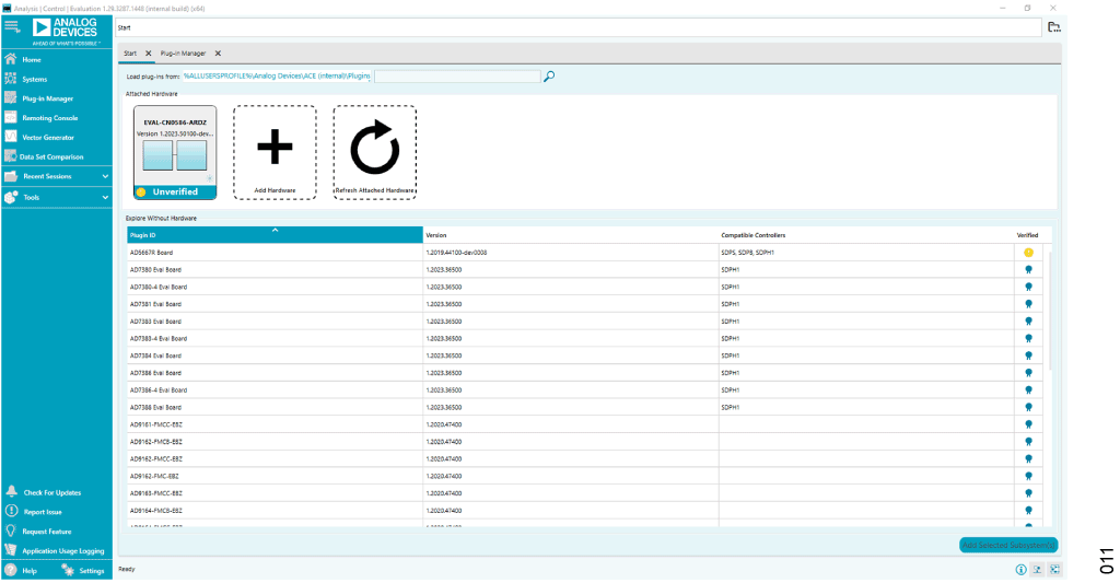
Figure 11. ACE Main Window.
- Double click the plugin to open the board view, as shown in Figure 12.
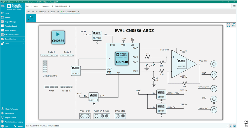
Figure 12. ACE Board View Window.
- Choose the desired "HV Output Range". Set "HV Out State" to "Enabled" and enter the desired HV output value.
Python can also be utilized to produce custom patterns or waveforms with the EVAL-CN0586-ARDZ. Figure 13 and Figure 14 show some sample waveforms produced using the python examples included in the design files of CN0586. Refer to the user guide for instructions on how set up python using PYADI-IIO.
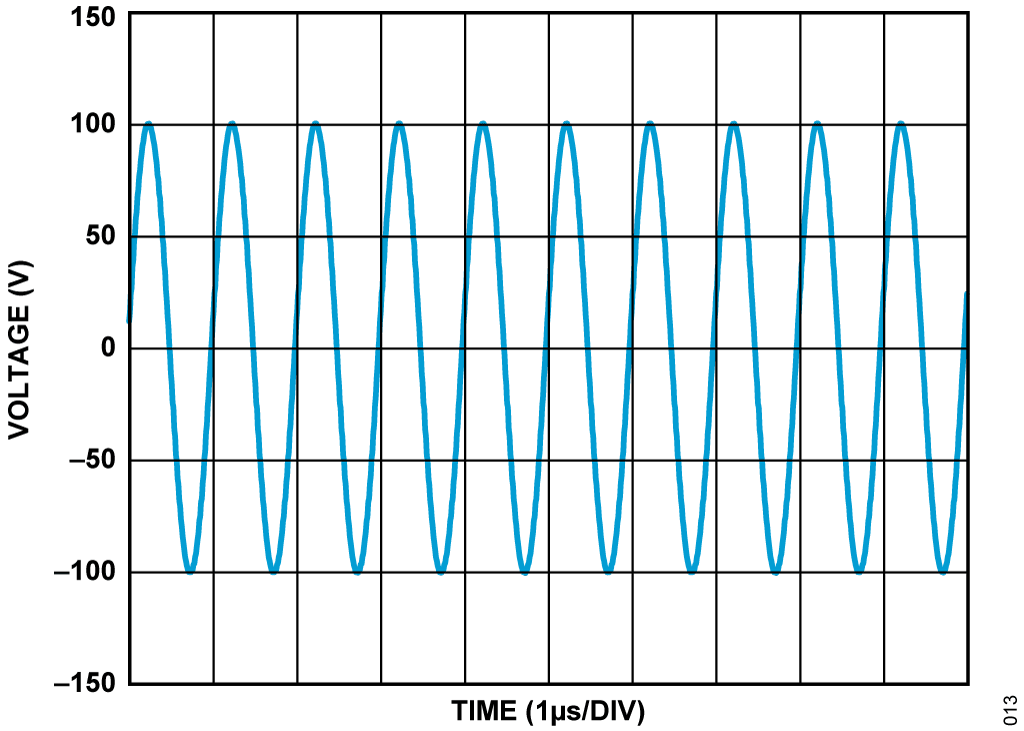
Figure 13. Sinewave Output Example.

Figure 14. Sweep Output Span Example.
