Design Solutions 1 - LTC2400 High Accuracy Differential to Single-Ended Converter for +-5V Supplies. Differential to Single-Ended Converter Has Very High Uncalibrated Accuracy and Low Offset and Drift
SPECIFICATIONS
| PARAMETER | CIRCUIT (MEASURED) | LTC2400 | TOTAL (UNITS) |
| Input Voltage Range | –3 to 40 | mV | |
| Zero Error | 12.7 | 1.5 | µV |
| Input Current | See Text | ||
| Nonlinearity | ±1 | 4 | ppm |
| Input-Referred Noise (without averaging) | 0.3* | 1.5 | µVRMS |
| Input-Referred Noise(averaged 64 readings) | 0.05* | µVRMS | |
| Resolution (with averaged readings) | 19.6 | Bits | |
| Overall Accuracy (uncalibrated**) | 18.1 | Bits | |
| Supply Voltage | ±5 | 5 | V |
| Supply Current | 1.6 | 0.2 | mA |
| CMRR | 120 | dB | |
| Common Mode Range | ±5 | V | |
| *Input-referred noise with a gain of 101. **Does not include gain setting resistors. |
|||
Operation
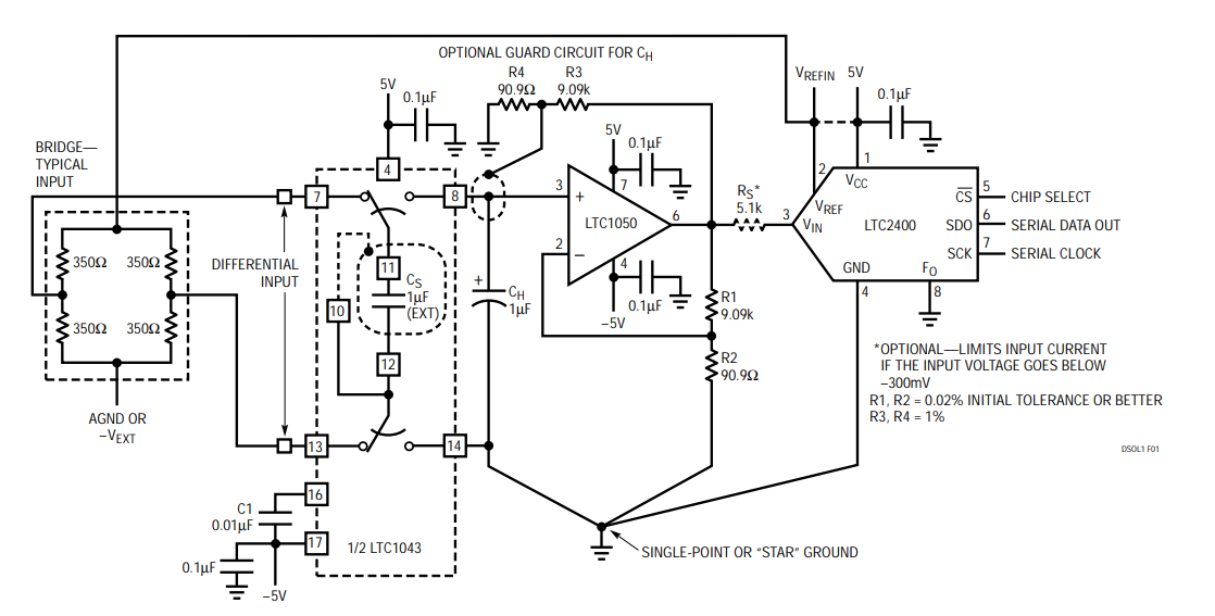
The circuit in Figure 1 is ideal for low level differential signals in applications that have a ±5V supply and need high accuracy without calibration. The circuit combines an LTC1043 and LTC1050 as a differential to single-ended amplifier that has an input common mode range that includes the power supplies. It uses the LTC1043 to sample a differential input voltage, holds it on CS and transfers it to a ground-referred capacitor, CH. The voltage on CH is applied to the LTC1050’s noninverting input and amplified by the gain set by resistors R1 and R2 (101 for the values shown). The amplifier’s output is then converted to a digital value by the LTC2400.

Figure 1. Differential to Single-Ended Converter for Low Level Inputs, Such as Bridges, Maintains the LTC2400’s High Accuracy.
The LTC1043 achieves its best differential to single-ended conversion when its internal switching frequency operates at a nominal 300Hz, as set by the 0.01µF capacitor C1 and when 1µF capacitors are used for CS and CH. CS and CH should be a film type such as mylar or polypropylene. Conversion accuracy is enhanced by placing a guard shield around CS and connecting the shield to Pin 10 of the LTC1043. This minimizes nonlinearity that results from stray capacitance transfer errors associated with CS. To minimize the possibility of PCB leakage currents introducing an error source into CH, an optional guard circuit could be added as shown. The common point of these two resistors produces the potential for the guard ring. Consult the LTC1043 data sheet for more information. As is good practice in all high precision circuits, keep all lead lengths as short as possible to minimize stray capacitance and noise pickup.
The LTC1050’s closed-loop gain accuracy is affected by the tolerance of the ratio of the gain-setting resistors. If cost considerations preclude using low tolerance resistors (0.02% or better), the processor to which the LTC2400 is connected can be used to perform software correction. Operated as a follower, the LTC1050’s gain and linearity error is less than 0.001%.
As stated above, the LTC1043 has the highest transfer accuracy when using 1.0µF capacitors. The input current is approximately –100nA at VIN(CM) = –5V, 100nA at VIN(CM) = 5V and 0µA at VIN(CM) = 0V. For example, 0.1µF will typically increase the circuit’s overall nonlinearity tenfold.
Another source of errors is thermocouple effects that occur in soldered connections. Their effects are most pronounced in the circuit’s low level portion, before the LTC1050’s output. Any temperature changes in any of the low level circuitry’s connections will cause linearity perturbations in the final conversion result. Their effects can be minimized by balancing the thermocouple connections with reversed redundant connections and by sealing the circuit against moving air.
A subtle source of error arises from ground lead impedance differences between the LTC1043 circuit, the LTC1050 preamplifier and the LTC2400. This error can be avoided by connecting Pin 14 of the LTC1043, the bottom end of R2 and Pin 4 of the LTC2400 to a single-point “star” ground.
The circuit’s input current is dependent on the input signal’s common mode voltage. The values may vary from part to part. Figure 1’s input is analogous to a 2µF capacitor in parallel with a 25MΩ connected to ground. The LTC1043’s nominal 800Ω switch resistance is between the source and the 2µF capacitance.
The circuit schematic shows an optional resistor, RS. This resistor can be placed in series with the LTC2400’s input to limit current if the input goes below –300mV. The resistor does not degrade the converter’s performance as long as any capacitiance, stray or otherwise, connected between the LTC2400’s input and ground is less than 100pF. Higher capacitance will increase offset and fullscale errors.
