资源库
EE-401: ADSP-SC5xx/215xx SHARC+ Processor System Optimization Techniques
Introduction
The ADSP-SC5xx/215xx SHARC+ processors (including both the ADSP-SC58x/2158x and ADSPSC57x/ADSP-215xx processor family) provide an optimized architecture supporting high system bandwidth and advanced peripherals. This application note discusses the key architectural features of the processors that contribute to the overall system bandwidth. It also discusses the available bandwidth optimization techniques.
Hereafter, the ADSP-SC5xx/215xx processors are called the ADSP-SC5xx processors; the ADSPSC58x/2158x processors are called ADSP-SC58x processors, and the ADSP-SC57x/2157x processors are called ADSP-SC57x processors. In the following sections, by default, the discussions refer to data measured on the ADSP-SC58x processor at 450 MHz CCLK (core clock) as an example. However, the concepts discussed also apply to the ADSP-SC58x processors at 500 MHz CCLK and the ADSP-SC57x processors at 450 MHz and 500 MHz CCLK operation. See the Appendix for the data corresponding to these modes of operation.
ADSP-SC5xx Processors Architecture
This section provides a holistic view of the key architectural features of the ADSP-SC5xx processors that play a crucial role in system bandwidth and performance. For detailed information about these features, refer to the ADSP-SC58x/ADSP-2158x SHARC+ Processor Hardware Reference1 for the ADSPSC58x/2158x processor family or the ADSP-SC57x/ADSP-2157x SHARC+ Processor Hardware Reference2 for the ADSP-SC57x processor family.
The overall architecture of ADSP-SC5xx processors primarily consists of three categories of system components: System Bus Slaves, System Bus Masters, and System Crossbars. Figure 1 and Figure 2 show how these components interconnect to form the complete system.
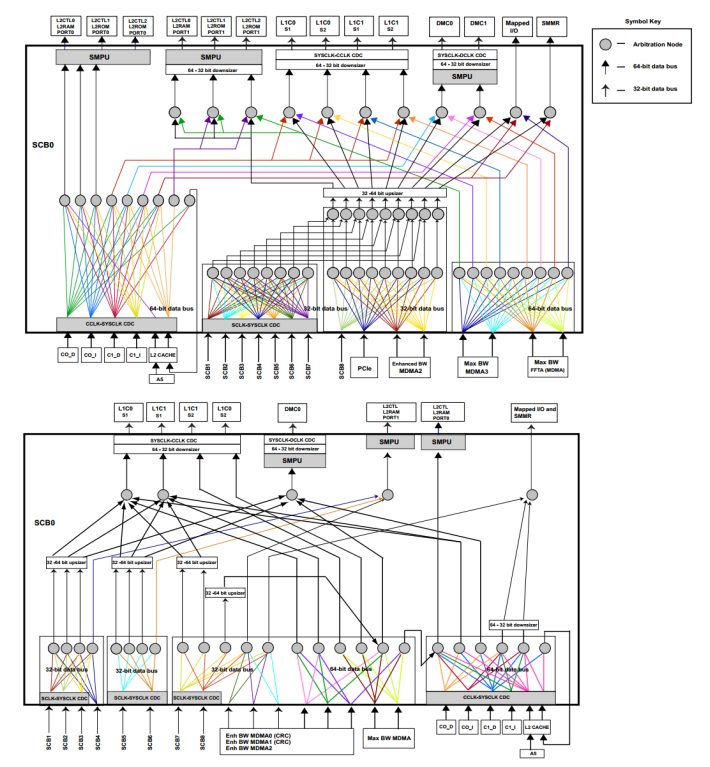
Figure 1. ADSP-SC58x (top) and ADSP-SC57x (bottom) System Cross Bar (SCB) Block Diagram.
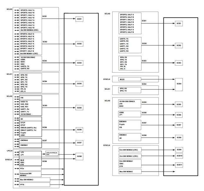
Figure 2. ADSP-SC58x (left) and ADSP-SC57x (right) SCB Master Groups.
System Bus Slaves
As shown at the top in Figure 1, System Bus Slaves include on-chip and off-chip memory devices and controllers such as:
- L1 SRAM
- L2 SRAM
- Dynamic Memory Controller (DMC) for DDR3/DDR2/LPDDR SDRAM devices
- Static Memory Controller (SMC) for SRAM and Flash devices
- Memory-mapped peripherals such as PCIe, SPI FLASH
- System Memory-Mapped Registers (MMRs)
Each System Bus Slave has its own latency characteristic and operates in a given clock domain. For example, L1 SRAM runs at CCLK, L2 SRAM runs at SYSCLK, the DMC (DDR3/DDR2/LPDDR) interface runs at DCLK and so on.
System Bus Masters
The System Bus Masters are shown at the bottom of Figure 1. The masters include peripheral Direct Memory Access (DMA) channels such as the Enhanced Parallel Peripheral Interface (EPPI) and Serial Port (SPORT) among others. The Memory-to-Memory DMA channels (MDMA) and the core are also included.
Note that each peripheral runs at a different clock speed, and thus has individual bandwidth requirements. For example, high speed peripherals such as Ethernet, USB, and Link Port require higher bandwidth than slower peripherals such as the SPORT, the Serial Peripheral Interface (SPI) and the Two Wire Interface (TWI).
System Crossbars
The System Crossbars (SCB) are the fundamental building blocks of the system bus interconnection. As shown in Figure 2, the SCB interconnect is built from multiple SCBs in a hierarchical model connecting system bus masters to system bus slaves. The crossbars allow concurrent data transfer between multiple bus masters and multiple bus slaves. This configuration provides flexibility and full-duplex operation. The SCBs also provide a programmable arbitration model for bandwidth and latency management. The SCBs run on different clock domains (SCLK0, SCLK1 and SYSCLK) that introduce their own latencies to the system.
System Optimization Techniques
The following sections describe how the System Bus Slaves, System Bus Masters, and System Crossbars affect system latencies and throughput and suggests ways to optimized throughput.
Understanding the System Masters
DMA Parameters
Each DMA channel has two buses; one bus connects to the SCB, which in turn is connected to the SCB
slave (for example, memories) and another bus connects to either a peripheral or another DMA channel.
The SCB and memory bus width varies between 8, 16, 32, or 64 bits and is defined by the DMA_STAT.MBWID bit field. The peripheral bus width varies between 8, 16, 32, 64, or 128 bits and is defined by the DMA_STAT.PBWID bit field. For ADSP-SC5xx processors, the memory and peripheral bus widths for most
of the DMA channels is 32 bits (4 bytes); for a few channels, it is 64 bits (8 bytes) wide. The DMA parameter DMA_CFG.PSIZE determines the width of the peripheral bus. It can be configured to 1,
2, 4, or 8 bytes. However, it cannot be greater than the maximum possible bus width defined by the DMA_STAT.PBWID bit field because burst transactions are not supported on the peripheral bus.
The DMA parameter DMA_CFG.MSIZE determines the actual size of the SCB bus in use. It also determines
the minimum number of bytes that are transferred to and from memory and correspond to a single DMA
request or grant. The parameter can be configured to 1, 2, 4, 8, 16, or 32 bytes. If the MSIZE value is greater
than DMA_STAT.MBWID, the SCB performs burst transfers to move the data equal to the MSIZE value.
It is important to understand how to choose the appropriate MSIZE value, both from a functionality and
performance perspective. Consider the following points when choosing the MSIZE value:
- The start address of the work unit must always align to the
MSIZEvalue selected. Failure to align generates a DMA error interrupt. - As a general rule, from a performance perspective, use the highest possible
MSIZEvalue (32 bytes) for better average throughput. This value results in a higher likelihood of uninterrupted sequential accesses to the slave (memory), which is the most efficient for typical memory designs. - From a performance perspective, in some cases, the minimum
MSIZEvalue is determined by the burst length supported by the memory device. For example, for DDR3 accesses, the minimumMSIZEvalue is limited by the DDR3 burst length (16 bytes). AnyMSIZEvalue below this limit leads to a significant throughput loss. For more details, refer to L3/External Memory Throughput.
Memory to Memory DMA (MDMA)
The ADSP-SC5xx processors support multiple MDMA streams (MDMA0/1/2/3) to transfer data from one memory to another (L1/L2/L3/memory-mapped peripherals including PCIe and SPI FLASH). Different MDMA streams are capable of transferring the data at varying bandwidths as they run at different clock speeds and support multiple data bus widths. Table 1 shows the MDMA streams and the corresponding maximum theoretical bandwidth supported by ADSP-SCxx processors at both 450 MHz and 500 MHz CCLK operation.
| Processor | MDMA Stream No. | MDMA Type | Maximum CCLK/SYSCLK/ SCLKx Speed (MHz) | MDMA Source Channel | MDMA Destination Channel | Clock Domain | Bus Width (bits) | Maximum Bandwidth (MB/s) |
|
ADSPSC58x 450 MHz Speed Grade
|
0 | Standard Bandwidth |
450/225/112.5
|
8 | 9 | SCLK0 |
32 | 450 |
| 1 | Standard Bandwidth | 18 | 19 | 32 | 450 | |||
| 2 | Enhanced Bandwidth or Medium Speed MDMA (MSMDMA) | 39 | 40 |
SYSCLK
|
32 | 900 | ||
| 3 | Maximum Bandwidth or High Speed MDMA (HSMDMA) | 43 | 44 | 64 | 1800 | |||
| 4 | FFT MDMA (when FFTA is disabled) | 41 | 42 | 64 | 1800 | |||
|
ADSPSC57x 450 MHz Speed Grade |
0 | Enhanced Bandwidth or Medium Speed MDMA (MSMDMA) | 8 | 9 | 32 | 900 | ||
| 1 | Enhanced Bandwidth or Medium Speed MDMA (MSMDMA) | 18 | 19 | 32 | 900 | |||
| 2 | Enhanced Bandwidth or Medium Speed MDMA (MSMDMA) | 39 | 40 | 32 | 900 | |||
| 3 | Maximum Bandwidth or High Speed MDMA (HSMDMA) | 43 | 44 | 64 | 1800 | |||
|
ADSPSC58x 500 MHz Speed Grade
|
0 | Standard Bandwidth |
500/250/125 |
8 | 9 | SCLK0 |
32 | 500 |
| 1 | Standard Bandwidth | 18 | 19 | 32 | 500 | |||
| 2 | Enhanced Bandwidth or Medium Speed MDMA (MSMDMA) | 39 | 40 |
SYSCLK |
32 | 1000 | ||
| 3 | Maximum Bandwidth or High Speed MDMA (HSMDMA) | 43 | 44 | 64 | 2000 | |||
| 4 | FFT MDMA (when FFTA is disabled) | 41 | 42 | 64 | 2000 | |||
|
ADSPSC57x 500 MHz Speed Grade
|
0 | Enhanced Bandwidth or Medium Speed MDMA (MSMDMA) | 8 | 9 | 32 | 1000 | ||
| 1 | Enhanced Bandwidth or Medium Speed MDMA (MSMDMA) | 18 | 19 | 32 | 1000 | |||
| 2 | Enhanced Bandwidth or Medium Speed MDMA (MSMDMA) | 39 | 40 | 32 | 1000 | |||
| 3 | Maximum Bandwidth or High Speed MDMA (HSMDMA) | 43 | 44 | 64 | 2000 |
Table 2 shows the memory slaves and the corresponding maximum theoretical bandwidth that the ADSPSC5xx processors support at both 450 MHz and 500 MHz CCLK operation.
| Processor | SHARC Core (C1/C2), Memory Type (L1/L2/L3), Port | Maximum CCLK/SYSCLK/SCLKx/DCLK Speed(MHz) | Clock Domain | Bus Width (bits) | Data Rate/Clock Rate | Maximum Theoretical Bandwidth (MB/s) |
|
ADSPSC58x 450 MHz Speed Grade |
C1L1S1 | 450/225/112.5/450 |
CCLK |
32 | 1 | 1800 |
| C1L1S2 | 32 | 1 | 1800 | |||
| C2L1S1 | 32 | 1 | 1800 | |||
| C2L1S2 | 32 | 1 | 1800 | |||
| L2 | SYSCLK | 32 | 1 | 900 | ||
| L3 | DCLK | 16 | 2 | 1800 | ||
| ADSPSC57x 450 MHz Speed Grade |
C1L1S1 | CCL |
32 | 1 | 1800 | |
| C1L1S2 | 32 | 1 | 1800 | |||
| C2L1S1 | 32 | 1 | 1800 | |||
| C2L1S2 | 32 | 1 | 1800 | |||
| L2 | SYSCLK | 64 | 1 | 1800 | ||
| L3 | DCLK | 16 | 2 | 1800 | ||
| ADSPSC58x 500 MHz Speed Grade |
C1L1S1 | 500/250/125/450 |
CCLK |
32 | 1 | 2000 |
| C1L1S2 | 32 | 1 | 2000 | |||
| C2L1S1 | 32 | 1 | 2000 | |||
| C2L1S2 | 32 | 1 | 2000 | |||
| L2 | SYSCLK | 32 | 1 | 1000 | ||
| L3 | DCLK | 16 | 2 | 1800 | ||
| ADSPSC57x 500 MHz Speed Grade |
C1L1S1 | CCLK |
32 | 1 | 2000 | |
| C1L1S2 | 32 | 1 | 2000 | |||
| C2L1S1 | 32 | 1 | 2000 | |||
| C2L1S2 | 32 | 1 | 2000 | |||
| L2 | SYSCLK | 64 | 1 | 2000 | ||
| L3 | DCLK | 16 | 2 | 1800 |
Refer to Table 1 and Table 2.
- The MDMA0 and MDMA1 streams on the ADSP-SC57x processors run at SYSCLK as compared with SCLK on ADSP-SC58x processors. Since SYSCLK is twice as fast as SCLK, ADSP-SC57x processor MDMA has twice the bandwidth of ADSP-SC58x processor MDMA.
- The DMA bus width for L2 memory on the ADSP-SC57x processors is 64 bits for HSMDMA as compared with 32 bits on the ADSP-SC58x processors. This bus width option facilitates better throughput for HSMDMA accesses to L2 memory in an ADSP-SC57x application.
The actual (measured) MDMA throughput is always less than or equal to the minimum of the maximum theoretical throughput supported by one of the three: MDMA, source memory, or destination memory. For example, the measured throughput of MDMA0 on the ADSP-SC58x processor between L1 and L2 is less than or equal to 450 MB/s. In this case, throughput is limited by the maximum bandwidth of MDMA0. Similarly, the measured throughput of MDMA3 between L1 and L2 on ADSP-SC58x processors is less than or equal to 900 MB/s. In this case, throughput is limited by the maximum bandwidth of L2.
Figure 3 shows measured throughput (for ADSP-SC58x processors at 450 MHz CCLK) for various MDMA
streams with different combinations of source and destination memories. The measurements were taken
with MSIZE
>
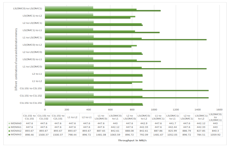
Figure 3. MDMA Throughput on ADSP-SC58x at 450 MHz CCLK.
Optimizing MDMA Transfers Not Aligned to 32-Byte Boundaries
In many cases, the start address and count of the MDMA transfer do not align with the 32-byte address
boundary. In this case, the conventional way is to configure the MSIZE value to less than 32 bytes which
might reduce the MDMA performance. To get better throughput, split the single MDMA transfer into more
than one transfer using descriptor-based DMA. Use MSIZE < 32 bytes for non 32-byte aligned address and count values for the first and last (if needed) MDMA transfers. Use MSIZE =32 bytes for 32-byte aligned
address and count values for the second transfer.
The example codes SC58x_MDMA_Memcpy_Core110 and SC57x_MDMA_Memcpy_Core10 provided with this application note illustrate how a 4-byte aligned MDMA transfer of 20000 bytes can be broken into three descriptor-based MDMA transfers. The first and third transfers use MSIZE =4 bytes and 4-byte aligned start address and count values. The second transfer uses MSIZE =32 bytes and 32-byte aligned start address and count values. The API Mem_Copy_MDMA() provided in the example code automatically calculates the required descriptor parameter values for these MDMA transfers for a given 4-byte aligned start address and count value.
Table 3 compares the cycles measured with the old and new MDMA methods for reading 20000 bytes from DDR3 from a 4-byte aligned start address. The numbers measured with the new MDMA method are much better (less than half) when compared with the old method.
| Processor |
Measured Core Cycles
|
|
| Old MDMA Method | New MDMA Method | |
| ADSP-SC589 | 33635 | 11711 |
| ADSP-SC573 | 32285 | 11261 |
Bandwidth Limiting and Monitoring
MDMA channels are equipped with a bandwidth limiting and monitoring mechanism. The bandwidth limiting feature can be used to reduce the number of DMA requests being sent by the corresponding masters to the SCB. In this section, SCLK/SYSCLK is used to convey the clock domain for the processor family being used (SCLK for ADSP-SC58x processors or SYSCLK for ADSP-SC57x processors).
The DMA_BWLCNT register can be programmed to configure the number of SCLK/SYSCLK cycles between two
DMA requests. This configuration ensures that the requests from the DMA channel do not occur more
frequently than required. Programming a value of 0x0000 allows the DMA to request as often as possible.
A value of 0xFFFF represents a special case and causes all requests to stop. The DMA_BWLCNT register and
the MSIZE value determine the maximum throughput in MB/s. The bandwidth is calculated as follows:
Bandwidth = min (SCLK/SYSCLK frequency in MHz*DMA bus width in bytes, SCLK/SYSCLK frequency in MHz*MSIZE
The example codes SC58x_MDMA_BW_Limit_Core1 and SC57x_MDMA_BW_Limit_Core110provided in
the associated .ZIP file utilize the MDMA3 stream to perform data transfers from DDR3 to L1 memory. In
this example, the DMC_BWLCNT register is programmed with different values to limit the throughput to a
maximum value for MSIZE values at the source/DDR3 end. Table 4 provides a summary of the theoretical
and measured throughput values (for ADSP-SC58x processors at 450 MHz CCLK) for different MSIZE and
BWLCNT values. As shown, the measured throughput is close to the theoretical bandwidth, which it never
exceeds. The SYSCLK frequency used for testing equals 225 MHz with a DMA buffer size of 16384 words.
Furthermore, the bandwidth monitor feature can be used to check if channels are starving for resources. The
DMC_BMCNT register can be programmed to the number of SCLK/SYSCLK cycles within which the
corresponding DMA must finish. Each time the DMA_CFG register is written to (MMR access only), a work
unit ends or an auto buffer wraps, the DMA loads the value in DMA_BWMCNT into DMA_BWMCNT_CUR. The DMA decrements DMA_BWMCNT_CUR every SCLK/SYSCLK that a work unit is active. If DMA_BWMCNT_CUR reaches 0x00000000 before the work unit finishes, the DMA_STAT.IRQERR bit is set and the DMA_STAT.ERRC
field is set to 0x6. The DMA_BWMCNT_CUR value remains at 0x00000000 until it is reloaded when the work
unit completes.
| Sample No. | MSIZE |
BWLCNT | Theoretical Throughput (MB/s) (SYSCLK*MSIZE/BWLCNT) | Measured Throughput (MB/s) |
| 1 | 32 | 8 | 900 | 787.36 |
| 2 | 32 | 16 | 450 | 422.22 |
| 3 | 32 | 32 | 225 | 217.83 |
| 4 | 32 | 64 | 112.5 | 110.68 |
| 5 | 32 | 128 | 56.25 | 55.79 |
| 6 | 16 | 8 | 450 | 398.92 |
| 7 | 16 | 16 | 225 | 211.46 |
| 8 | 16 | 32 | 112.5 | 109.01 |
| 9 | 16 | 64 | 56.25 | 55.36 |
| 10 | 16 | 128 | 28.125 | 27.9 |
| 11 | 8 | 8 | 225 | 199.73 |
| 12 | 8 | 16 | 112.5 | 105.81 |
| 13 | 8 | 32 | 56.25 | 54.53 |
| 14 | 8 | 64 | 28.125 | 27.69 |
| 15 | 8 | 128 | 14.0625 | 13.95 |
Unlike other error sources, a bandwidth monitor error does not stop the work unit from processing. Programming 0x00000000 disables the bandwidth monitor functionality. This feature can also be used to measure the actual throughput.
Example code (SC58x_MDMA_BW_Monitor_Core110 and SC57x_MDMA_BW_Monitor_Core110) is provided
in the associated .ZIP file to help explain this functionality. The example uses the MDMA3 stream
configured to read from DDR3 memory to L1 memory. The DMC_BWMCNT register is programmed to 4096
for an expected throughput of 900 MB/s (Buffer Size*SYSCLK speed in MHz/Bandwidth =
16384*225/900).
When this MDMA runs alone, the measured throughput (both using cycle count and DMC_BWMCNT) appears as expected (1060 MB/s). The output is shown in Figure 4.

Figure 4. Using DMC_BWMCNT for Measuring Throughput.
Using the same example code, if another DMC read MDMA2 stream is initiated in parallel (#define ADD_ANOTHER_MDMA), the throughput drops to less than 900 MB/s and a bandwidth monitor error is generated. Figure 5 shows the error output when the bandwidth monitor expires due to less than expected throughput.

Figure 5. Bandwidth Monitor Error.
Extended Memory DMA (EMDMA)
The ADSP-SC5xx processors also support Extended Memory DMA (EMDMA). This feature was called an External Port DMA (EPDMA) on previous SHARC processors. The EMDMA engine is mainly used to transfer the data from one memory type to another in a non-sequential manner (such as circular, delay line, scatter and gather, and so on).
For details regarding EMDMA, refer to the ADSP-SC58x/ADSP-2158x SHARC+ Processor Hardware Reference1 for the ADSP-SC58x processor family or the ADSP-SC57x/ADSP-2157x SHARC+ Processor Hardware Reference2 for the ADSP-SC57x processor family.
Figure 6 shows the measured throughput (for ADSP-SC58x processors at 450 MHz CCLK) for EMDMA0
and EMDMA1 streams with different combinations of source and destination memories for sequential
transfers. The measurements were taken with MSIZE =32 bytes and DMA count =16384 bytes. For the
corresponding measurements for ADSP-SC58x processors at 500 MHz CCLK and ADSP-SC57x
processors at 450MHz and 500 MHz CCLK, refer to Figure 22, Figure 23, and Figure 24 in the Appendix.
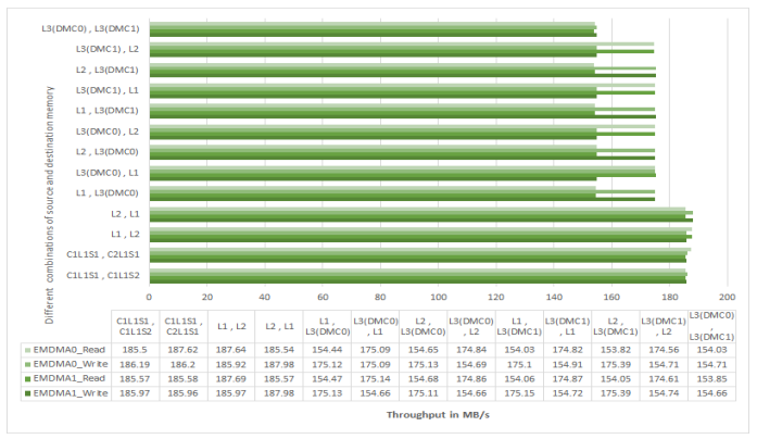
Figure 6. EMDMA Throughput on ADSP-SC58x Processors at 450 MHz CCLK.
As shown, the EMDMA throughput for sequential transfers is significantly less when compared to the MDMA transfers. For improved performance, use MDMA instead of EMDMA for sequential transfers.
Optimizing Non-Sequential EMDMA Transfers with MDMA
In some cases, the non-sequential transfer modes supported by EMDMA can be replaced by a descriptorbased MDMA for better performance.
The SC58x_Circular_Buffer_MDMA_Core110 and SC57x_Circular_Buffer_MDMA_Core110 examples illustrate how MDMA descriptor-based mode can be used to emulate circular buffer memory-to-memory DMA transfer mode supported by EMDMA to achieve higher performance. The example code compares the core cycles measured (see Table 5) to write and read 4096 32-bit words to and from the DDR3 memory in circular buffer mode with a starting address offset of 1024 words for the following three cases:
- EMDMA
- MDMA with
MSIZE=4 bytes (for 4-byte aligned address and count) - MDMA with
MSIZE=32 bytes (for 32-byte aligned address and count)
Table 5 shows that the MDMA emulated circular buffer (MSIZE =4 bytes) is much faster than EMDMA.
The performance is further improved with MSIZE =32 bytes if the addresses and counts are 32-byte aligned.
| Processor |
Write/Read |
Core Cycles |
||
| EMDMA |
MDMA3 MSIZE 4 bytes | MDMA3 MSIZE 32 bytes |
||
| ADSP-SC58x |
Write | 46210 | 25150 | 6194 |
| Read | 50288 | 27589 | 8051 | |
| ADSP-SC57x |
Write | 46272 | 22568 | 5534 |
| Read | 50288 | 26485 | 7753 | |
Understanding the System Crossbars
As shown in Figure 2, the SCB interconnect consists of a hierarchical model connecting multiple SCB units. Figure 7 shows the block diagram for a single SCB unit. It connects the System Bus Masters (M) to the System Bus Slaves (S) using a Slave Interface (SI) and Master Interface (MI). On each SCB unit, each S is connected to a fixed MI. Similarly, each M is connected to a fixed SI.

Figure 7. Single SCB Block Diagram.
The slave interface of the crossbar (where the masters such as DDE connect) performs two functions: arbitration and clock domain conversion.
Arbitration
Programmable Quality of Service (QoS) registers are associated with each SCB. For example, the QoS registers for SPORT0, 1, 2, 3, and MDMA0 can be viewed as residing in SCB1. Whenever a transaction is received at SPORT0 half A, the programmed QoS value is associated with that transaction and is arbitrated with the rest of the masters at SCB1.
Programming the SCB QOS Registers
Consider a scenario where:
- At SCB1, masters 1, 2, and 3 have RQOS values of 6, 4, and 2, respectively
- At SCB2, masters 4, 5, and 6 have RQOS values of 12, 13, and 1, respectively

Figure 8. Arbitration Example.
In this case:
- Master 1 wins at SCB1 due to its highest RQOS value of 6, and master 5 wins at SCB2 due to its highest RQOS value of 13.
- In a perfect competition at SCB0, masters 4 and 5 have the highest overall RQOS values. So, they would fight for arbitration directly at SCB0. Because of the mini-SCBs, however, master 1, at a much lower RQOS value, is able to win against master 4 and continue to SCB0.
Clock Domain Conversion
There are multiple clock domain crossings available in the ADSP-SC5xx system fabric including:
- CCLK to SYSCLK
- SCLK to SYSCLK
- SYSCLK to CCLK
- SYSCLK to DCLK.
The clock domain crossing SYSCLK to DCLK is programmable for both of the DMC interfaces. Program this clock domain crossing based on the clock ratios of the two clock domains for optimum performance.
Programming Sync Mode in the IBx Registers
To illustrate the effect of the sync mode programming in the IBx registers, DDR3 read throughput was measured with an MDMA3 stream at CCLK=450 MHz, SCLK0/1=112.5 MHz, SYSCLK=225 MHz, DCLK=450 MHz. Figure 9 shows DMC MDMA throughput with and without IBx sync mode programming. The throughput was measured (for ADSP-SC58x processors) for two cases:
- SYSCLK: DCLK CDC programmed in ASYNC (default) mode
- SYSCLK: DCLK CDC programmed in SYNC (1:n) mode
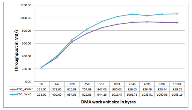
Figure 9. DMC MDMA Throughput.
Refer to Figure 25 in the Appendix for data corresponding to the ADSP-SC57x processors. For 500 MHz CCLK operation, the CDC can only be programmed to ASYNC mode.
As shown, the throughput improves when the CDC is programmed in SYNC mode as compared with ASYNC mode.
Understanding the System Slave Memory Hierarchy
As shown in Table 2, the ADSP-SC5xx processors have a hierarchical memory model (L1-L2-L3). The following sections discuss the access latencies and optimal throughput associated with the different memory levels.
L1 Memory Throughput
L1 memory runs at CCLK and is the fastest accessible memory in the hierarchy. Each SHARC+ core have its own L1 memory that is accessible by both the core and DMA (system). For system (DMA) accesses, L1 memory supports two ports (S1 and S2). Two different banks of L1 memory can be accessed in parallel using these two ports.
Unlike ADSP-SC58x processors, on the ADSP-SC57x processors all the system (DMA) accesses are hardwired to access the L1 memory of the SHARC+ core through the S1 port except for the High Speed MDMA (HSMDMA). HSMDMA is hardwired to access the memory through the S2 port. From a programming perspective, when accessing the L1 memory of the SHARC+ core through DMA, only use the S1 port multiprocessor memory offset (0x28000000 for SHARC+ core 1 and 0x28800000 for SHARC+ core 2) for HSMDMA.
The maximum theoretical throughput of L1 memory (for system/DMA accesses) is 450*4=1800 MB/s for 450 MHz CCLK operation and 500*4 = 2000 MB/s for 500 MHz CCLK operation. As shown in Figure 3, Figure 19, Figure 20, and Figure 21, the maximum measured L1 throughput using MDMA3 for both ADSPSC58x and ADSP-SC57x processors is approximately 1500 MB/s for 450 MHz CCLK operation. For 500 MHz CCLK operation, it is approximately 1667 MB/s for ADSP-SC58x processors and approximately 1974 MB/s for ADSP-SC57x processors.
L2 Memory Throughput
L2 memory access times are longer than L1 memory access times because the maximum L2 clock frequency is half the CCLK, which equals the SYSCLK. The L2 memory controller contains two ports to connect to the system crossbar. Port 0 is a 64-bit wide interface dedicated to core traffic, while port 1 is a 32-bit wide interface that connects to the DMA engine (ADSP-SC57x processors support a 64-bit DMA bus for HSMDMA accesses). Each port has a read and a write channel. For details, refer to the ADSP-SC58x/ADSP2158x SHARC+ Processor Hardware Reference1 or ADSP-SC57x/ADSP-2157x SHARC+ Processor Hardware Reference1 .
Consider the following points for L2 memory throughput:
- Since L2 memory runs at the SYSCLK rate, it is capable of providing a maximum theoretical throughput of 225 MHz*4 = 900 MB/s in one direction (for ADSP-SC57x processor HSMDMA accesses, it can go up to 1800 MB/s). Because there are separate read and write channels, the total throughput in both directions equals 1800 MB/s. Use both core and DMA ports and separate read and write channels in parallel to operate L2 SRAM memory at its optimum throughput. The core, ports and channels should access different banks of L2.
- All accesses to L2 memory are converted to 64-bit accesses (8 bytes) by the L2 memory controller. Thus, in order to achieve optimum throughput for DMA access to L2 memory, configure the DMA channel MSIZE to 8 bytes or higher.
- Unlike L3 (DMC) memory accesses, L2 memory throughput for sequential and non-sequential accesses is the same.
- L2 SRAM is ECC-protected and organized into eight banks. A single 8- or 16-bit access, or a non32-bit address-aligned 8-bit or 16-bit burst access to an ECC-enabled bank creates an additional latency of two SYSCLK cycles. This latency is because the ECC implementation is in terms of 32 bits. Any writes that are less than 32 bits wide to an ECC-enabled SRAM bank are implemented as a read followed by a write and requires three cycles to complete (two cycles for the read, one cycle for the write).
- When performing simultaneous core and DMA accesses to the same L2 memory bank, use read and write priority control registers to increase the DMA throughput. If both the core and DMA access the same bank, the best access rate that DMA can achieve is one 64-bit access every three SYSCLK cycles during the conflict period. Program the read and write priority count bits (
L2CTL_RPCR.RPC0andL2CTL_WPCR.WPC0) to 0, while programming theL2CTL_RPCR.RPC1andL2CTL_WPCR.WPC1bits to 1 to maximize the throughput.
Figure 10 shows measured MDMA throughput (for ADSP-SC58x processors at 450 MHz CCLK) for a case
where both source and destination buffers are in different L2 memory banks. It shows L2 MDMA
throughput for different MSIZE and work unit size values. For MDMA2, the maximum throughput is close
to 900 Mbytes/sec in one direction (=1800 Mbytes/s in both directions) for all MSIZE settings above and
equal to 8 bytes. Throughput drops significantly for an MSIZE of 4 bytes.
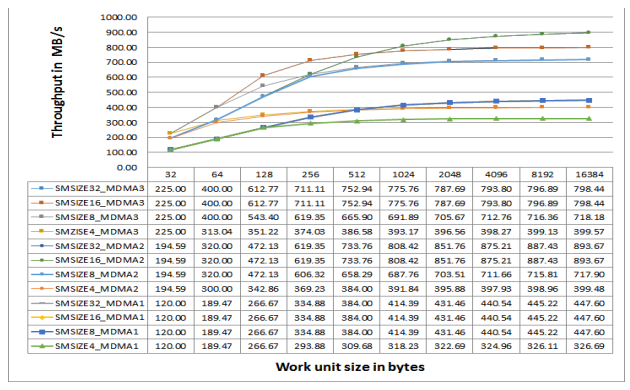
Figure 10. L2 MDMA Throughput vs. Work Unit Size.
Refer to Figure 26, Figure 27, and Figure 28 in the Appendix for the corresponding measurements for ADSP-SC58x processors at 500 MHz CCLK and ADSP-SC57x processors at 450MHz and 500 MHz CCLK.
L3/External Memory Throughput
ADSP-SC5xx processors provide interfaces for connecting to different types of off-chip L3 memory devices, such as the Static Memory Controller (SMC) for interfacing to parallel SRAM/Flash devices and the Dynamic Memory Controller (DMC) for connecting to DRAM (DDR3/DDR2/LPDDR) devices.
The DMC interface operates at speeds of up to 450 MHz for DDR3 mode. Thus, for the 16-bit DDR3 interface, the maximum theoretical throughput which the DMC can deliver equals 1800 MB/s. However, the practical maximum DMC throughput is less due to:
- latencies introduced by the internal system interconnects, and
- latencies that are derived from the DRAM technology itself (access patterns, page hit-to-page miss ratio, and so on.)
There are techniques for achieving optimum throughput when accessing L3 memory through the DMC. Although most of the throughput optimization concepts are illustrated using MDMA as an example, the same concepts can be applied to other system masters as well.
The MDMA3 stream (HSMDMA) can request DMC accesses faster than any other masters (for example, 1800 MB/s). The DMC throughput using MDMA depends upon factors such as:
- whether the accesses are sequential or non-sequential
- the block size of the transfer
- DMA parameters (such as MSIZE).
Figure 11 and Figure 12 provide the measured DMC throughput (for ADSP-SC58x processors at 450 MHz CCLK) using MDMA1 (channels 18/19), MDMA2 (channels 39/40), and MDMA3 (channels 43/44) streams for various MSIZE values and buffer sizes between L1 and L3 memories for sequential read and write accesses, respectively. For the corresponding measurements for ADSP-SC58x processors at 500 MHz CCLK and ADSP-SC57x processors at 450MHz and 500 MHz CCLK, refer to the Figures 29-34 in the Appendix.
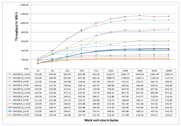
Figure 11. DMC Throughput for Sequential MDMA Reads.
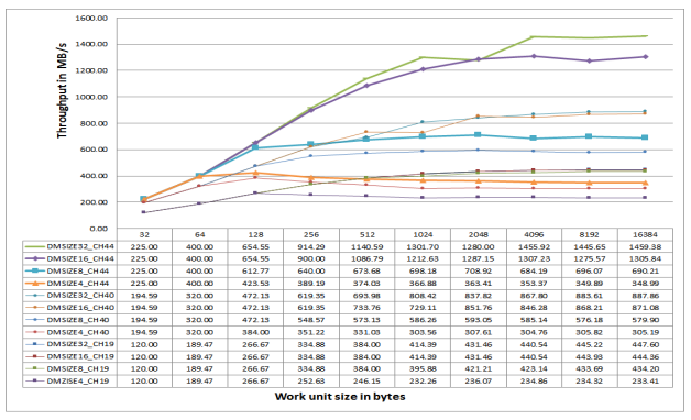
Figure 12. DMC Throughput for Sequential MDMA Writes.
Consider the following important observations:
- The throughput trends are similar for reads and writes with regard to
MSIZEand buffer size values. - The peak measured read throughput is 1147.34 MB/s for MDMA3 channel 43 with
MSIZE= 16 bytes The peak measured write throughput is 1459.38 MB/s for MDMA3 channel 44 withMSIZE= 32 bytes. - The throughput depends largely upon the DMA buffer size. For smaller buffer sizes, the throughput
is significantly lower. Throughput increases significantly with a larger buffer size. For instance,
DMA channel 43 with an
MSIZEof 32 bytes and a buffer size of 32 bytes has a read throughput of 225 MB/s. The throughput reaches 1064.51 MB/s with a 16 Kbyte buffer size. This increase is largely due to the overhead incurred when programming the DMA registers, as well as the system latencies when sending the initial request from the DMA engine to the DMC controller.
Arrange the DMC accesses such that the DMA count is as large as possible to improve sustained throughput for continuous transfers over time.
- To some extent, throughput depends upon the
MSIZEvalue of the source MDMA channel for reads and destination MDMA channel for writes. As shown in Figures 11 and Figure 12, in most cases, greaterMSIZEvalues provide better results. Ideally, theMSIZEvalue is at least equal to the DDR memory burst length. For MDMA channel 43 with a buffer size of 16384 bytes, the read throughput is 1064.51 MB/s for anMSIZEof 32 bytes. The throughput reduces significantly to 220.27 MB/s for anMSIZEof 4 bytes. AlthoughMSIZEis 4 bytes and all accesses are sequential, the full DDR3 memory burst length of 16 bytes (eight 16-bit words) is not used.
For sequential reads, it is possible to achieve optimum throughput, particularly for larger buffer sizes. This optimal state can happen because the DRAM memory page hit ratio is high and the DMC controller does not need to close and open DDR device rows too often. However, in the case of non-sequential accesses, throughput can drop slightly or significantly depending upon the page hit-to-miss ratio.
Figure 13 shows a comparison of the DMC throughput numbers measured for sequential MDMA read
accesses for an MSIZE of 16 bytes (equal to the DDR3 burst length), and the ADDRMODE bit set to 0 (bank
interleaving) versus non-sequential accesses with a modifier of 2048 bytes (equal to the DDR3 page size,
thus leading to a worst-case scenario with maximum possible page misses). As shown, for a buffer size of
16384 bytes, throughput drops significantly from 1148.41 to 306.89 MB/s.
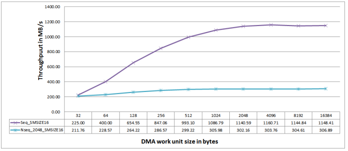
Figure 13. DMC Throughput for Non-Sequential and Sequential Read Access.
DDR memory devices support concurrent bank operation allowing the DMC controller to activate a row in
another bank without pre-charging the row of a particular bank. This feature is extremely helpful in cases
where DDR access patterns result in page misses. By setting the DMC_CTL.ADDRMODE bit, throughput can be improved by ensuring that such accesses fall into different banks. For instance, Figure 14 shows (in red), how the DMC throughput increases from 306.89 MB/s to 546.94 MB/s by setting this bit for the nonsequential access pattern shown in Figure 13.
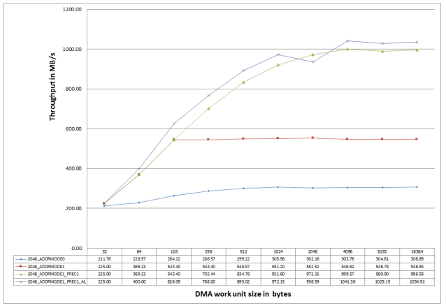
Figure 14. Optimizing Throughput for Non-Sequential Accesses.
The throughput can be improved using the DMC_CTL.PREC bit, which forces the DMC to close the row automatically as soon as a DDR read burst is complete using the Read with Auto Precharge command. The row of a bank proactively precharges after it has been accessed. The action improves the throughput by saving the latency involved in precharging the row when the next row of the same bank must be activated.
This functionality is illustrated (the green line) in Figure 14. Note how the throughput increases from 546.94 MB/s to 996.59 MB/s by setting the DMC_CTL.PREC bit. The same result can be achieved by setting the DMC_EFFCTL.PRECBANK[7-0] bits. This feature can be used on per bank basis. However, note that setting the DMC_CTL.PREC bit overrides the DMC_EFFCTL_PRECBANK[7-0] bits. Also, setting the DMC_CTL.PREC bit results in the precharging of the rows after every read burst, while setting the DMC_EFFCTL_PRECBANK[7-0] bits precharges the row after the last burst corresponding to the respective MSIZE settings. This configuration provides an added throughput advantage for cases where MSIZE (for example, 32 bytes) is greater than the DDR3 burst length (16 bytes).
For reads, use the additive latency feature supported by the DMC controller and DDR3/DDR2 SDRAM devices (TN47029) to improve throughput as shown in Figure 15 and Figure 16. Although the figures are shown for DDR2, the same concept applies to DDR3 devices.

Figure 15. DDR2 Reads Without Additive Latency.

Figure 16. DDR2 Reads With Additive Latency.
Programming the additive latency to tRCD-1 allows the DMC to send the Read with Autoprecharge
command immediately after the Activate command and before tRCD completes. This enables the controller
to schedule the Activate and Read commands for other banks, eliminating gaps in the data stream. The
purple line in Figure 14 shows how the throughput improves from 996.59 MB/s to 1034.92 MB/s by
programming the additive latency (AL) in the DMC_EMR1 register to tRCD-1 (equals 5 or CL-1 in this case).
The DMC also allows elevating the priority of the accesses requested by a particular SCB master with the
DMC_PRIO and DMC_PRIOMSK registers. The associated .ZIP file provides example code (SC58x_DMC_SCB_PRIO_Core110 and SC57x_DMC_SCB_PRIO_Core110) in which two MDMA DMC read
channels (8 and 18) run in parallel. Table 6 summarizes the measured throughout.
| Test Case Number | Priority Channel (SCB ID) | MDMA0 (Ch 8) Throughput (MB/s) | MDMA1 (Ch 18) Throughput (MB/s) |
| 1 | None | 363 | 363 |
| 2 | MDMA0(0x008) | 388 | 342 |
|
3 |
MDMA1(0x208) | 321 | 356 |
For test case 1, when no priority is selected, the throughput for both MDMA channel 8 and 18 is 363 MB/s.
MDMA channel 8 throughput increases to 388 MB/s by setting the DMC_PRIO register to the corresponding
SCB ID (0x008) and the DMC_PRIOMSK register to 0xFFFF. Similarly, MDMA channel 18 throughput
increases to 356 MB/s by setting the DMC_PRIO register to the corresponding SCB ID (0x208) and the
DMC_PRIOMSK register to 0xFFFF.
Furthermore, the Postpone Autorefresh command can be used to ensure that auto-refresh commands do not interfere with any critical data transfers. Up to eight Autorefresh commands can accumulate in the DMC. Program the exact number of Autorefresh commands using the NUM_REF bit in the DMC_EFFCTL register.
After the first refresh command accumulates, the DMC constantly looks for an opportunity to schedule a refresh command. When the SCB read and write command buffers become empty (which implies that no access is outstanding) for the programmed number of clock cycles (IDLE_CYCLES) in the DMC_EFFCTLregister, the accumulated number of refresh commands are sent back to back to the DRAM memory.
After every refresh, the SCB command buffers are checked to ensure that they remain empty. However, if the SCB command buffers are always full, once the programmed number of refresh commands accumulates, the refresh operation is elevated to an urgent priority and one refresh command is sent immediately. After this, the DMC continues to wait for an opportunity to send out refresh commands. If self-refresh is enabled, all pending refresh commands are given out only after that DMC enters self-refresh mode.
There is a slight increase in the MDMA3 DMC read throughput from 1063.90 MB/s to 1077.26 MB/s after enabling the postpone auto-refresh feature for MSIZE = 32 bytes and a DMA count of 16 K bytes.
System MMR Latencies
Unlike previous SHARC processors, the ADSP-SC5xx SHARC+ processors can have higher MMR access latencies. This is mainly due to the interconnect fabric between the core and the MMR space, and also due to the number of different clock domains (SYSCLK, SCLK0, SCLK1, DCLK and CAN clock). The ADSPSC5xx processors have five groups of peripherals for which the MMR latency varies, as shown in Table 7 and Table 8.
| Group 1 |
Group 2 | Group 3 | Group 4 | Group 5 | ||
| SPORT | ASRC | TMU | L2CTL | SPI2 | CAN | DMC |
| UART | CRC | HADC | CGU | EPPI | ||
| SPI | SPDIF_RX | USB | RCU | |||
| TWI | DMA 8/18/28/38 | FIR | SEC | |||
| ACM | PORT | IIR | CDU | |||
| EMAC | PADS | RTC | DPM | |||
| MLB | PINT | WDOG | MDMA2/3 | |||
| EMDMA | SMC | DAI | DEBUG | |||
| MSI | SMPU | SINC | FFT | |||
| SPDIF_TX | COUNTER | SWU | TRU | |||
| LP | PWM | TIMER | SPU | |||
| PCG | OTPC | |||||
| Group 1 |
Group 2 | Group 3 | Group 4 | Group 5 | ||
| SPORT | SPDIF_RX | DAI | L2CTL | SPI2 | CAN | DMC |
| UART | PORT | SINC | CGU | |||
| SPI | PADS | SWU | RCU | |||
| TWI | PINT | SEC | ||||
| ACM | SMC | CDU | ||||
| EMAC | SMPU | DPM | ||||
| TIMER | COUNTER | MDMA2/3 | ||||
| EMDMA | WDOG | DEBUG | ||||
| MSI | ZOTPC | TRU | ||||
| SPDIF_TX | TMU | SPU | ||||
| LP | HADC | DMA8/18/28/38 | ||||
| PCG | USB | MEC0 | ||||
| EEPI | FIR | MLB | ||||
| ASRC | IIR | CRC | ||||
Table 9 and Table 10 show the approximate MMR access latency CCLK cycles for the different groups of peripherals. Across the group, the peripherals observe similar MMR access latencies.
| Processor Family | MMR Access | Group 1 | Group 2 | Group 3 | Group 4 | Group 5 |
| ADSP-SC58x |
MMR Read | 84 | 66 | 80 | 225 | 74 |
| MMR Write | 44 | 33 | 43 | 159 | 42 | |
| ADSP-SC57x |
MMR Read | 90 | 66 | 88 | 225 | 78 |
| MMR Write | 64 | 59 | 42 | 160 | 69 |
| Processor Family | MMR Access | Group 1 | Group 2 | Group 3 | Group 4 | Group 5 |
| ADSP-SC58x |
MMR Read | 58 | 42 | 56 | 190 | 54 |
| MMR Write | 58 | 41 | 55 | 182 | 56 | |
| ADSP-SC57x |
MMR Read | 58 | 45 | 53 | 181 | 55 |
| MMR Write | 57 | 42 | 59 | 191 | 55 |
The MMR latency numbers are measured along with the “sync” (SHARC+ core) and “dsb” (ARM core) instructions after the write. This operation ensures that the write has taken affect. Both SHARC+ and ARM cores support posted writes, which means that the core does not necessarily
However, the MMR access latencies can vary depending upon the following factors:
- Clock ratios: All MMR accesses are through SCB0, which is in the SYSCLK domain, while peripherals are in the SCLK0/1, SYSCLK, and DCLK domains.
- Number of concurrent MMR access requests in the system: Although a single write incurs half the system latency as compared with back-to-back writes, the latency observed on the core is shorter. Similarly, the system latency incurred by a read followed by a write (or a write followed by a read) is different than the latency observed on the core.
- Memory type: where the code is executed from (L1/L2/L3).
System Bandwidth Optimization Procedure
Although the optimization techniques can vary from one application to another, the general procedure involved in the overall system bandwidth optimization remains the same. Figure 17 provides a flow chart of a typical system bandwidth optimization procedure for ADSP-SC5xx-based applications.
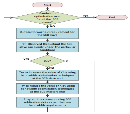
Figure 17. Typical System Bandwidth Optimization Flow.
A typical procedure for an SCB slave includes the following steps:
- Identify the individual and total throughput requirements by all the masters accessing the corresponding SCB slave in the system and allocate the corresponding read/write SCB arbitration slots accordingly. Consider the total throughput requirement as X.
- Calculate the observed throughput that the corresponding SCB slave(s) is able to supply under the specific conditions. Refer to this as Y.
For X<Y, the bandwidth requirements are met. For X>Y, one or more peripherals are likely to hit a reduced throughput or underflow condition. In this case, apply the bandwidth optimization techniques as discussed in earlier sections to either:
- Increase the value of Y by applying the slave-specific optimization techniques (for example, use the DMC efficiency controller features), or
- Decrease the value of X by:
- Reanalyzing whether a particular peripheral needs to run fast. If not, then slow down the peripheral to reduce the bandwidth requested by the peripheral.
- Reanalyzing whether a particular MDMA can be slowed down. Use the corresponding
DMAx_BWLCNTregister to limit the bandwidth of that particular DMA channel.
Application Example
Figure 18 shows a block diagram of the example application code supplied with this EE-Note for an ADSPSC58x processor at 450 MHz CCLK. Refer to Figure 35 in the Appendix for the block diagram that corresponds to an ADSP-SC57x processor at 450 MHz CCLK.
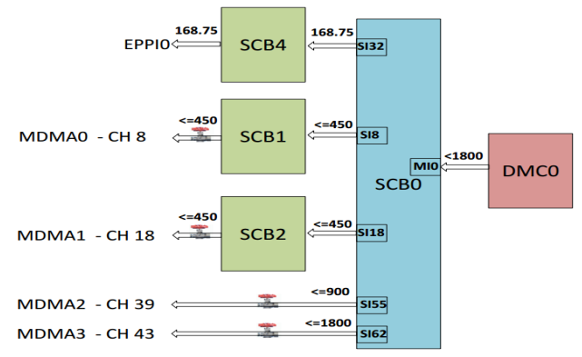
Figure 18. DMC Throughput Distribution Across SCBs.
The code supplied emphasizes the use of the SCBs and the DMC controller for high throughput requirements and shows the various bandwidth optimization techniques. Throughput does not depend on pin multiplexing limitations.
The example code has the following conditions/requirements:
- CCLK=450 MHz, DCLK = 450 MHz, SYSCLK = 225 MHz, SCLK0 = SCLK1 = 112.5 MHz
- EPPI0 (SCB4): 24-bit transmit, internal clock and frame sync mode at EPPICLK = 56.25 MHz, required throughput = 56.25 MHz * 3 = 168.75 MB/s.
- MDMA0 channel 8, required throughput = 112.5 MHz * 4 ≤ 450 MB/s.
- MDMA1 channel 18, required throughput = 112.5 MHz * 4 ≤ 450 MB/s
- MDMA2 channel 39, required throughput = 225 MHz * 4 ≤ 900 MB/s
- MDMA3 channel 43, required throughput = 225 MHz * 8 ≤ 1800 MB/s
Throughput requirements for the MDMA channels depend on the corresponding DMAx_BWLCNT register
values. If not programmed, the MDMA channels request the bandwidth with full throttle.
As shown in Figure 18, the total required throughput from the DMC controller equals 3768.75 MB/s.
Theoretically, with DCLK = 450 MHz and a bus width of 16 bits, the maximum possible throughput is 1800
MB/s. For this reason, there is a possibility that one or more masters do not get the required bandwidth. For
masters such as MDMA, this situation can result in decreased throughput. For other masters such as EPPI,
it can result in an underflow condition.
Table 11 shows the expected and measured throughput (for an ADSP-SC58x processor at 450 MHz CCLK) for all DMA channels and the corresponding SCBs at various steps of bandwidth optimization. For an ADSP-SC57x processor at 450 MHz CCLK measurements, refer to Table 12 in the Appendix.
| S. No. |
Condition |
SCB4 |
SCB1 |
SCB2 |
MDMA2 |
MDMA3 |
Total throughput Requirement X |
Measured throughput Y' |
PPI Underflow? |
|||||
| PPIO |
MDMA0 |
MDMA1 |
||||||||||||
| Required | Measured | Required | Measured | Required | Measured | Required | Measured | Required | Measured | |||||
| 1 | No Optimization | 168.375 | 145.05 | 450 | 99.29 | 450 | 98.64 | 900 | 167.29 | 1800 | 260.43 | 3768.75 | 770.7 | YES |
| 2 | Optimization at the slave - T1 | 168.375 | 170 | 450 | 182.93 | 450 | 182.22 | 900 | 362.12 | 800 | 566.79 | 2768.75 | 1464.06 | NO |
| 3 | Optimization at the master - T2 | 168.375 | 170 | 200 | 189.48 | 200 | 189.3 | 330 | 330.411 | 550 | 524.67 | 1448.75 | 1403.861 | NO |
| 4 | Optimization at the master - T3 | 168.375 | 170.29 | 100 | 97.55 | 100 | 97.29 | 300 | 292.94 | 780 | 752.63 | 1448.75 | 1410.7 | NO |
| All units are expressed in MBytes/sec. | ||||||||||||||
Step 1
In this step, all DMA channels run without applying any optimization techniques. To replicate the worst case scenario, the source buffers of all DMA channels are placed in a single DDR3 SDRAM bank. The row corresponding to No optimization in Table 11 shows the measured throughput numbers under this condition. As illustrated, the individual measured throughput of almost all channels is significantly less than expected and all EPPIs show an underflow condition
- Total expected throughput from the DMC (X) = 3768.75 MB/s
- Effective DMC throughput (Y) = 770.7 MB/s
Clearly, X is greater than Y which demonstrates a need for implementing the recommended bandwidth optimization techniques
Step 2
When frequent DDR3 SDRAM page misses occur within the same bank, throughput drops significantly. Although DMA channel accesses are sequential, page misses are likely to occur because multiple channels attempt to access the DMC concurrently. To work around this, move the source buffers of each DMA channel to different DDR3 SDRAM banks. This configuration allows parallel accesses to multiple pages of different banks and thereby improves Y. The row labeled Optimization at the slave - T1 in Table 11 provides the measured throughput numbers under this condition. Both individual and overall throughput numbers increase significantly. The maximum throughput delivered by the DMC (Y) increases to 1464.06 MB/sec and the EEPI0 underflow disappears. However, since X is still greater than Y, the measured throughput is still lower than expected.
Step 3 and 4
There is not much more room to significantly increase the value of Y. Alternatively, optimization techniques can be employed at the master end. Depending on the application requirements, the bandwidth limit feature of the MDMAs can be used to reduce the overall bandwidth requirement and to get a predictable bandwidth at various MDMA channels. The rows Optimization at the master - T2 and Optimization at the master – T3 in Table 11 show the measured throughput under two such conditions with different bandwidth limit values for the various MDMA channels. As shown, the individual and total throughput are very close to the required throughput; no underflow conditions exist.
System Optimization Techniques – Checklist
This section summarizes the optimization techniques discussed in this application note. It also includes some additional tips for bandwidth optimization.
- Analyze the overall bandwidth requirements and use the bandwidth limit feature for memory pipe DMA channels to regulate the overall DMA traffic.
- Program the optimal
MSIZEparameter for the DMA channels to maximize throughput and avoid any potential underflow or overflow conditions. - If required and possible, split a single MDMA transfer having a lower
MSIZEvalue into multiple descriptor-based MDMA transfers to increase theMSIZEvalue for better performance. - Use MDMA instead of EMDMA for sequential data transfers to improve performance. When possible, emulate EMDMA non-sequential transfer modes with MDMA to improve performance.
- Program the SCB
RQOSandWQOSregisters to allocate priorities to various masters, as per system requirements. - Program the clock domain crossing (
IBx) registers depending upon the clock ratios across SCBs. - Use optimization techniques at the SCB slave end, such as:
- Efficient usage of the DMC controller
- Usage of multiple L2/L1 sub-banks to avoid access conflicts
- Usage of instruction and data caches
- Maintain the optimum clock ratios across different clock domains
- Since MMR latencies affect the interrupt service latency, the ADSP-SCxx processors feature the Trigger Routing Unit (TRU) for bandwidth optimization and system synchronization. The TRU allows for synchronizing system events without processor core intervention. It maps the trigger masters (trigger generators) to trigger slaves (trigger receivers), thereby off-loading processing from the core. For a detailed discussion on this, refer to Utilizing the Trigger Routing Unit for System Level Synchronization (EE-360)8. Although the EE-Note is written for the ADSPBF60x processors, the concepts apply to the ADSP-SC5xx processors too.
Appendix
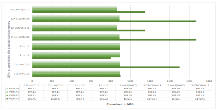
Figure 19. MDMA Throughput on ADSP-SC57x Processors at 450 MHz CCLK.
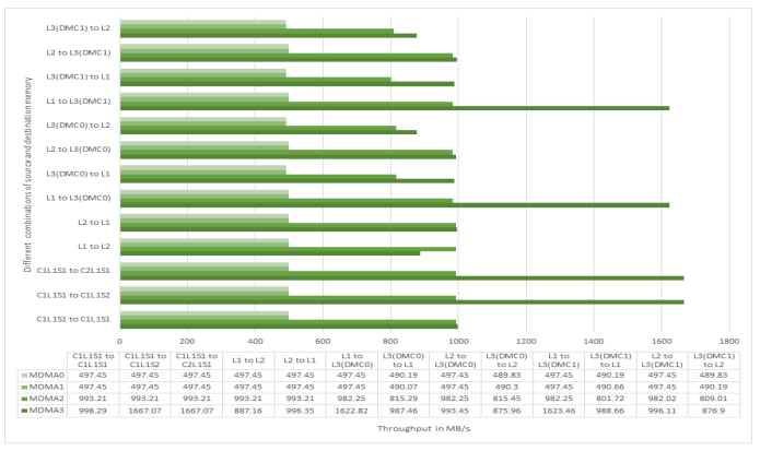
Figure 20. MDMA Throughput on ADSP-SC58x Processors at 500 MHz CCLK.
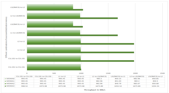
Figure 21. MDMA Throughput on ADSP-SC57x Processors at 500 MHz CCLK.
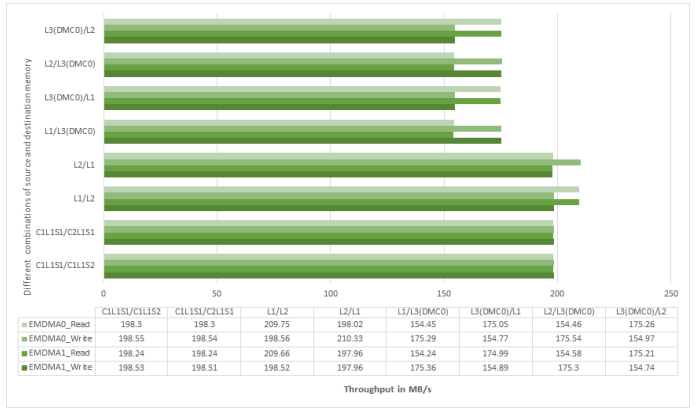
Figure 22. EMDMA Throughput on ADSP-SC57x Processors at 450 MHz CCLK.
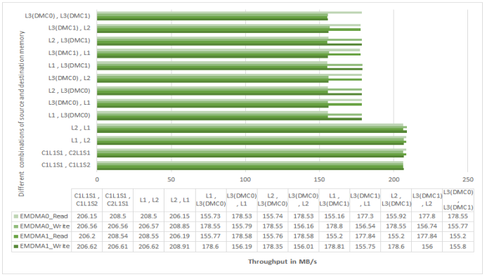
Figure 23. EMDMA Throughput on ADSP-SC58x Processors at 500 MHz CCLK.
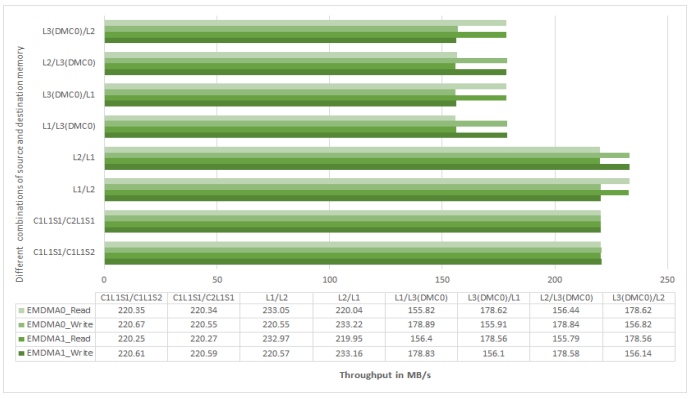
Figure 24. EMDMA Throughput on ADSP-SC57x Processors at 500 MHz CCLK.
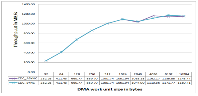
Figure 25. DMC MDMA Throughput on ADSP-SC57x Processors at 450 MHz CCLK (with and without IBx sync mode programming).
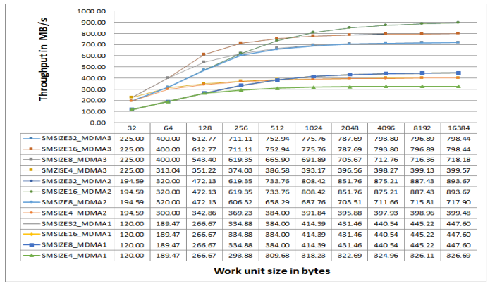
Figure 26. L2 MDMA Throughput on ADSP-SC57x Processors at 450 MHz CCLK.
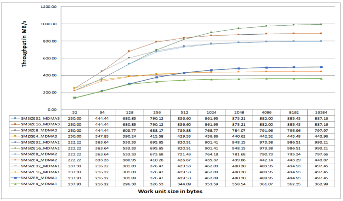
Figure 27. L2 MDMA Throughput on ADSP-SC58x Processors at 500 MHz CCLK.
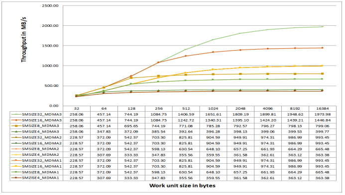
Figure 28. L2 MDMA Throughput on ADSP-SC57x Processors at 500 MHz CCLK.
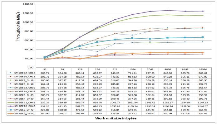
Figure 29. DMC Throughput for Sequential MDMA Reads on ADSP-SC57x Processors at 450 MHz CCLK.
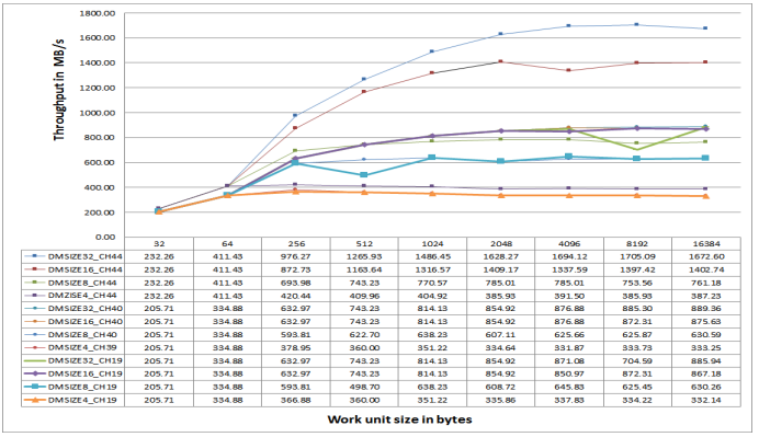
Figure 30. DMC Throughput for Sequential MDMA Writes on ADSP-SC57x Processors at 450 MHz CCLK.
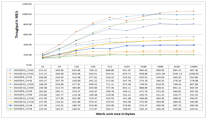
Figure 31. DMC Throughput for Sequential MDMA Reads on ADSP-SC58x Processors at 500 MHz CCLK.
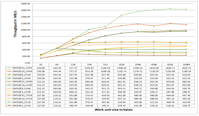
Figure 32. DMC Throughput for Sequential MDMA Writes on ADSP-SC58x Processors at 500 MHz CCLK.
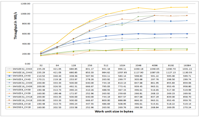
Figure 33. DMC Throughput for Sequential MDMA Reads on ADSP-SC57x Processors at 500 MHz CCLK.
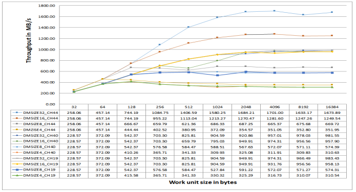
Figure 34. DMC Throughput for Sequential MDMA Writes on ADSP-SC57x Processors at 500 MHz CCLK.
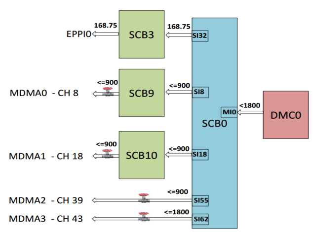
Figure 35. DMC Throughput Distribution Example for ADSP-SC57x Processors at 450 MHz CCLK.
| S. No. |
Condition |
SCB3 |
SCB9 |
SCB10 |
MDMA2 |
MDMA3 |
Total throughput Requirement X |
Measured throughput Y' |
PPI Underflow? |
|||||
| PPIO |
MDMA0 |
MDMA1 |
||||||||||||
| Required | Measured | Required | Measured | Required | Measured | Required | Measured | Required | Measured | |||||
| 1 | No optimization | 168.75 | 170 | 900 | 146.84 | 900 | 146.79 | 900 | 146.83 | 1800 | 146.83 | 4668.75 | 757.29 | NO |
| 2 | Optimization at the slave - T1 | 168.75 | 170 | 900 | 454.94 | 900 | 455.17 | 900 | 455.11 | 1800 | 170.51 | 4668.75 | 1705.73 | NO |
| 3 | Optimization at the master - T2 | 168.75 | 170 | 200 | 194.76 | 200 | 194.96 | 300 | 289.74 | 1000 | 820 | 1868.75 | 1669.46 | NO |
| 4 | Optimization at the master - T3 | 168.75 | 170 | 400 | 380 | 400 | 380.08 | 400 | 379.29 | 500 | 345.82 | 1868.75 | 1655.19 | NO |
参考电路
- ADSP-SC58x/ADSP-2158x SHARC+ Processor Hardware Reference. Rev 1.0, September 2017. Analog Devices, Inc.
- ADSP-SC57x/ADSP-2157x SHARC+ Processor Hardware Reference. Rev 0.2, June 2017. Analog Devices, Inc.
- ADSP-SC582/SC583/SC584/SC587/SC589/ADSP-21583/21584/21587 SHARC+ Dual Core DSP with ARM Cortex-A5 Processor Data Sheet. Rev A, July 2017. Analog Devices, Inc.
- ADSP-SC572/SC573/ADSP-21573 SHARC+ Dual Core DSP with ARM Cortex-A5 Processor Data Sheet. Rev 0, June 2017. Analog Devices, Inc.
- ADSP-BF60x Blackfin® Processors System Optimization Techniques (EE-362). Rev 1, November 2013. Analog Devices, Inc.
- ADSP-BF70x Blackfin+® Processors System Optimization Techniques (EE-376). Rev 1, January 2016
- System Optimization Techniques for Blackfin® Processors (EE-324). Rev 1, July 2007. Analog Devices, Inc.
- Utilizing the Trigger Routing Unit for System Level Synchronization (EE-360). Rev 1, October 2013. Analog Devices, Inc.
- TN-47-02: DDR2 Offers New Features/Functionality Introduction. Rev A, June 2006. Micron Technology Inc.
- Associated ZIP File for ADSP-SC5xx/215xx SHARC+ Processor System Optimization Techniques (EE-401). Rev 1, February 2018. Analog Devices, Inc.

