AN-2641: Fast, Efficient, and Compact: LT7153SP for Modern Optical Transceiver Power Rails
Introduction
Next-generation optical modules used in data centers and telecom networks continue to push the limits of power density, efficiency, and signal integrity. As link speeds increase from 100G to 800G and beyond, module designers face stringent constraints on printed circuit board (PCB) area, thermal performance, and electromagnetic interference (EMI), while still requiring fast, accurate power delivery to support high-speed digital signal processors (DSPs), lasers, transimpedance amplifiers (TIAs), and serializer-deserializer (SerDes) circuits. The LT7153SP, a 5V, ±25A monolithic step-down regulator with Silent Switcher® 2 technology, is specifically engineered to address these challenges. Its compact footprint, ultralow EMI performance, excellent transient response, and support for multiphase operation make it well-suited for modern optical modules, where board space is limited and performance margins are critical.
LT7153SP Specifications
LT7153SP is an innovative power management solution that delivers high efficiency, best-in-class thermal performance, and fast load-transient response. These attributes are essential for today’s communication systems, datacenter equipment, and compact optical module designs, where power density, heat dissipation, and transient accuracy directly affect system performance and reliability. The key specifications and design considerations for the LT7153SP are described in the following sections.
Solution Size
The overall solution height is primarily determined by the inductor, as the LT7153SP device and its associated input/output capacitors are relatively low-profile components. Although an inductor with lower DC resistance (DCR) generally improves efficiency by reducing conduction loss, it often requires a larger footprint or greater height, which can be challenging in height-restricted applications such as optical modules.
To meet strict Z-height constraints, a parallel-inductor approach is used. Instead of a single SLC7649S-500 (50nH) inductor with a 4.6 mm height, two XGL4020-101 (100nH) inductors are placed in parallel. This configuration reduces the maximum height to 1.2mm, satisfying the mechanical requirements of optical-module customers.
The two parallel inductors connect to a common SW node and conduct simultaneously without phase interleaving. Consequently, this configuration does not provide the current-ripple cancellation benefits associated with multiphase operation. However, the parallel inductors effectively share the AC and DC, reduce core/AC losses per inductor, and provide a compact, thermally balanced solution while meeting strict height limitations.
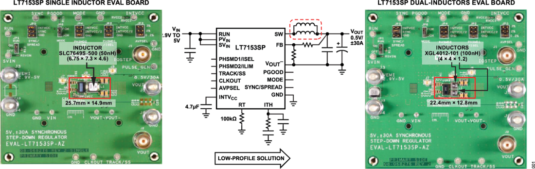
The demonstration circuit EVAL-LT7153SP-AZ supports both single-inductor and dual-inductor configurations using a common footprint. The default assembly uses a single 70nH SLC7649S-700KLC inductor. For applications with stringent Z-height constraints, such as optical modules, the board can be readily reconfigured to use two low-profile inductors in parallel while maintaining the same effective inductance.
Efficiency and Thermal Performance
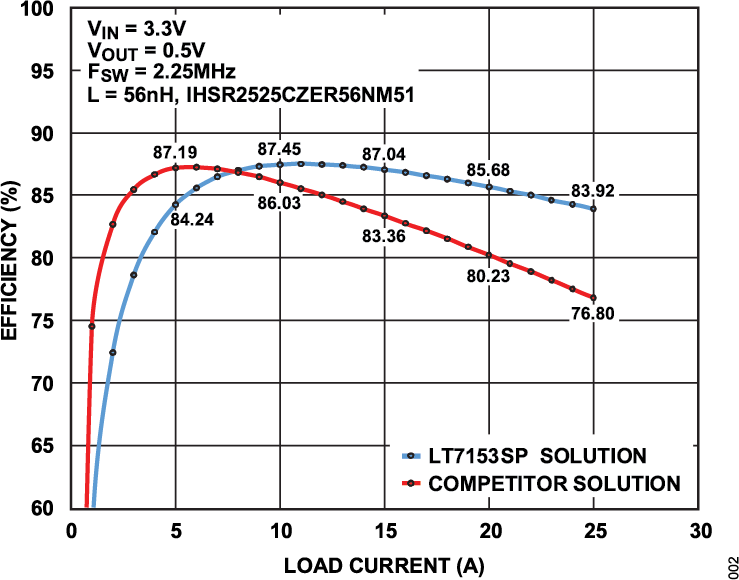
The LT7153SP delivers high efficiency and best-in-class thermal performance, which are critical for minimizing temperature rise in compact optical module environments. Figure 2 illustrates an efficiency comparison between the LT7153SP and a competing solution under identical test conditions. At the full-load rating of 25A, the LT7153SP achieves approximately 7% higher efficiency than the competitor’s device, significantly reducing system power loss.
At an output current of 25A, the LT7153SP solution reduces power loss by 0.88W per optical module. In a large-scale AI rack containing a thousand optical modules, this translates to approximately 880W of power savings per rack, significantly reducing the power and cooling demands of modern data centers.
This efficiency advantage translates directly into superior thermal performance. As shown in Figure 3, the device exhibits a temperature rise of approximately 30 °C, whereas the competing solution shows a temperature rise of approximately 75 °C under the same operating conditions. This large thermal gap provides practical system-level benefits: with the LT7153SP, additional cooling elements—such as heat sinks or airflow enhancements—are typically unnecessary, even at elevated ambient temperatures. In contrast, the competitor’s device may require supplemental thermal management to maintain reliable operation in thermally constrained environments.
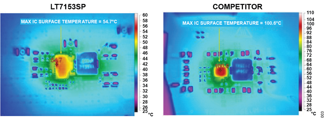
The combination of high efficiency and low thermal rise makes the LT7153SP an excellent fit for power-dense optical modules, where temperature budget, reliability, and long-term performance are tightly constrained.
Output Voltage Ripple
In optical modules, the digital signal processor (DSP) and high-speed analog front end handle the transmission and reception of multi-gigabit data streams. These circuits are highly sensitive to supply noise, making it essential to deliver a low-ripple, low-noise power rail to prevent interference and maintain signal integrity. The LT7153SP provides exceptionally low output ripple in a compact footprint, making it well-suited for these noise-sensitive applications.
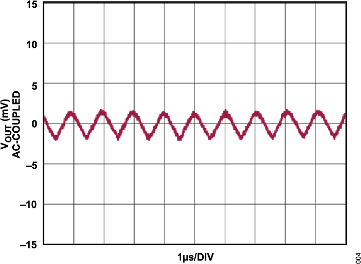
Figure 4 shows an example of the LT7153SP output ripple operating at VIN = 3.3 V, VOUT = 0.5 V, and IOUT = 25A. The output stage uses five 100μF (0805) ceramic capacitors and four 22μF (0402) capacitors to achieve high effective capacitance with low equivalent series resistance (ESR) and equivalent series inductance (ESL). Given these conditions, the measured peak-to-peak ripple is less than 5mV, demonstrating the LT7153SP’s capability to deliver a clean, stable power rail even at high load currents. This performance is critical for maintaining reliable operation in high-speed optical module systems.
Fixed Frequency Constant On-Time Control for Fast Load Transient
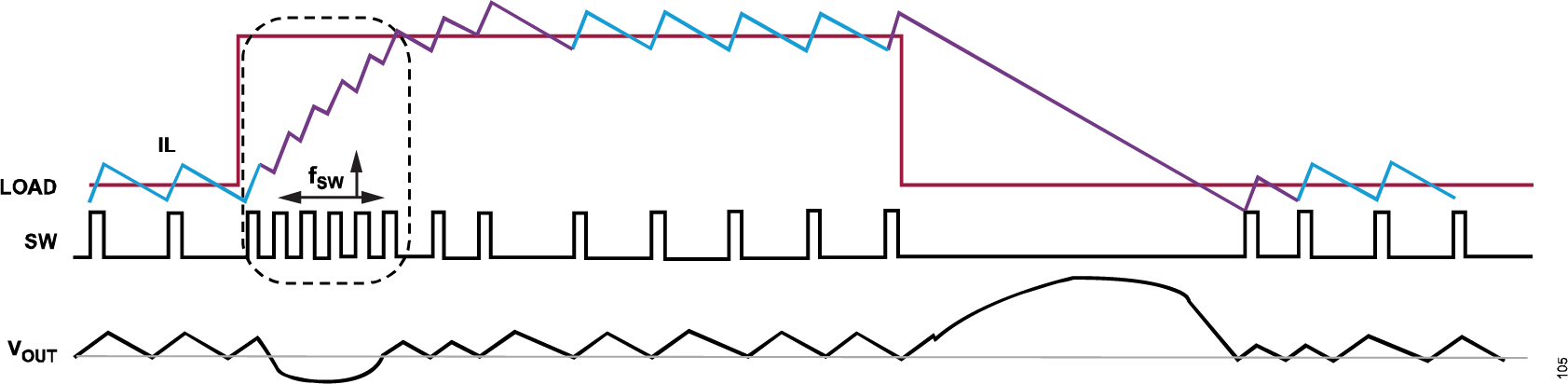
The LT7153SP uses a fixed-frequency, constant-on-time (COT) control architecture that combines the fast transient response of COT control with the predictable switching characteristics of a fixed-frequency converter. This architecture is well suited for high-current, space-constrained applications such as optical modules, where stringent EMI requirements and excellent dynamic performance during rapid load transients are critical.
Traditional fixed-frequency PWM controllers, such as peak-current-mode designs, maintain a constant switching frequency under all operating conditions. While this behavior simplifies EMI management, it introduces clock latency during fast load transients because the controller cannot adjust the duty cycle until the next switching cycle. This delay can increase output-voltage deviation during large, high-slew-rate load steps.
The LT7153SP’s fixed-frequency constant-on-time (FF COT) architecture overcomes this limitation. During steady-state operation, the device maintains a stable switching frequency through a phase-locked loop (PLL) that derives it from VIN, VOUT, and the user-programmed switching frequency. However, during transient conditions, FF COT operates as a true constant-on-time controller, responding immediately to output deviations without waiting for the clock.
Group of Pulses on Load Step-Up
During a load step-up event, the output voltage momentarily dips as current demand rises. The LT7153SP's valley voltage or current comparator detects this droop and immediately triggers a group of on-time pulses without waiting for the fixed-frequency clock cycle. This near-instantaneous response rapidly increases inductor current and delivers the required energy to the load, significantly reducing output droop and improving transient recovery time.
Extended Off Time or Pulse Skipping on Load Step-Down
During a load step decrease, the inductor current can temporarily exceed the load demand, causing output-voltage overshoot. To mitigate this condition, the LT7153SP automatically extends the off-time or skips switching pulses, allowing the inductor current to decay rapidly to the new steady-state value. This adaptive response minimizes output overshoot and limits excess energy delivered to the output capacitors.
Silent Switcher® 2 Enables Ultralow EMI Performance
Another key advantage of the LT7153SP is its integration of Silent Switcher® 2 technology, which delivers ultralow EMI without compromising efficiency or transient response. This is critical for optical modules and high-speed communications equipment, where switching noise can interfere with sensitive optical receivers, SerDes lanes, or RF circuits. Silent Switcher® 2 minimizes both radiated and conducted emissions through several architectural enhancements:
- High-di/dt switching loops are the primary source of radiated EMI. Silent Switcher® 2 integrates the critical input capacitors directly within the device package, placing them near the power switches. This dramatically shrinks the hot-loop area and reduces high-frequency magnetic fields at the source.
- By embedding critical layout elements on-chip, Silent Switcher® 2 eliminates layout-dependent variability and maintains low EMI performance on dense PCB layouts, enabling robust implementation in optical module form factors.
- Traditional low-EMI techniques slow the switch-node transition, often at the expense of efficiency. Silent Switcher® 2 instead relies on optimized geometry and loop minimization, enabling fast transitions and high efficiency while still achieving excellent EMI performance.
In summary, Silent Switcher® 2 enables the LT7153SP to deliver high-current, high-efficiency power conversion with ultralow EMI, even in dense optical module environments. When used in a polyphase configuration, the LT7153SP provides a scalable, low-noise power architecture ideally suited for next-generation optical transceivers and other noise-sensitive communication systems.
Target Applications for Optical Module Customer Design
With its excellent efficiency and thermal performance, the LT7153SP has gained strong adoption among optical-module designers. These systems typically require multiphase power converters to supply the core rail of high-speed DSPs and application-specific integrated circuits (ASICs), where efficiency and thermal behavior are top priorities due to limited power budgets and airflow within the module. In addition to electrical performance, optical-module customers enforce strict constraints on solution size, especially maximum component height, and place high importance on reliability features.
The following sections present a multiphase LT7153SP design optimized for these requirements and demonstrate how the device addresses the efficiency, thermal, size, and reliability challenges of next-generation optical modules.
Multiphase Dual Inductors for Low-Profile Designs
A single LT7153SP can deliver up to 25A of output current. For applications requiring higher load capability, multiple LT7153SP devices can be connected in parallel to form a multiphase power stage, improving efficiency, reducing ripple, and distributing thermal load. To support these higher-current optical-module applications, a multiphase LT7153SP evaluation board has been developed with a compact, low-profile design optimized for height-restricted environments.
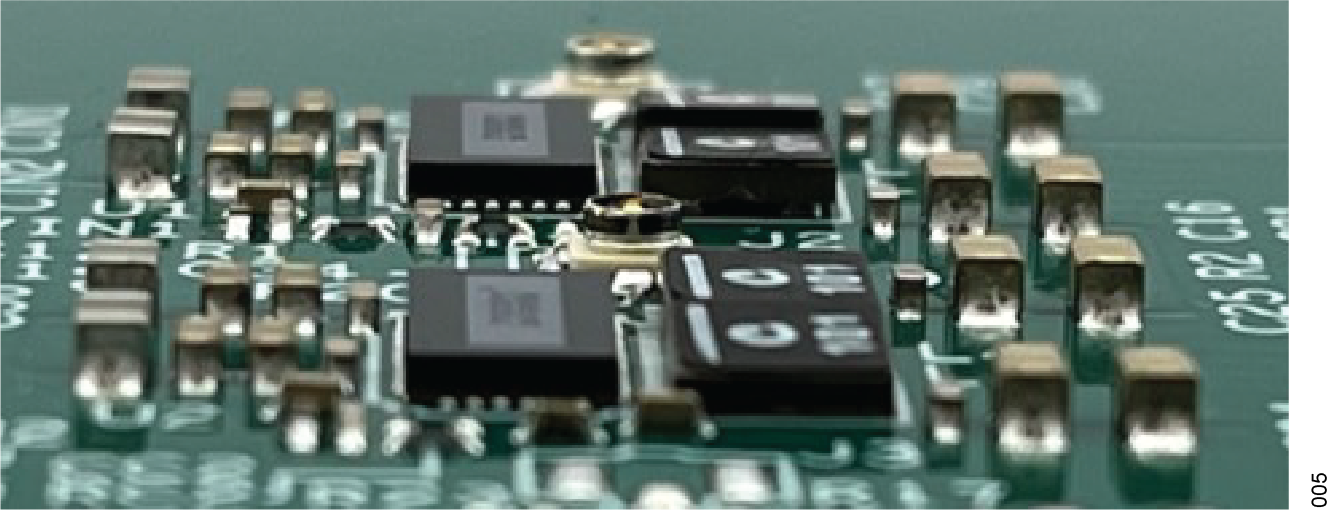
The design uses XGL4012-101MEC inductors (4mm × 4mm × 1.2mm), enabling a significantly lower Z-height compared to standard inductor options. As shown in Figure 6, the 2-phase LT7153SP solution employs dual inductors per phase, to reduce the overall solution height while maintaining the required inductance and current-handling capability. This dual-inductor approach is particularly valuable for optical-module customers, where height is often one of the most restrictive mechanical constraints.
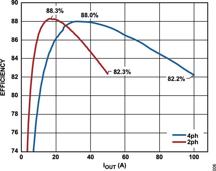
In the 2-phase configuration, the LT7153SP achieves a peak efficiency of 88.3%, with 82.3% efficiency at a full 50A load. For applications requiring even higher current, a 4-phase LT7153SP implementation can supply up to 100A, delivering a peak efficiency of 88.0% and 82.2% efficiency at full load, as shown in Figure 7.
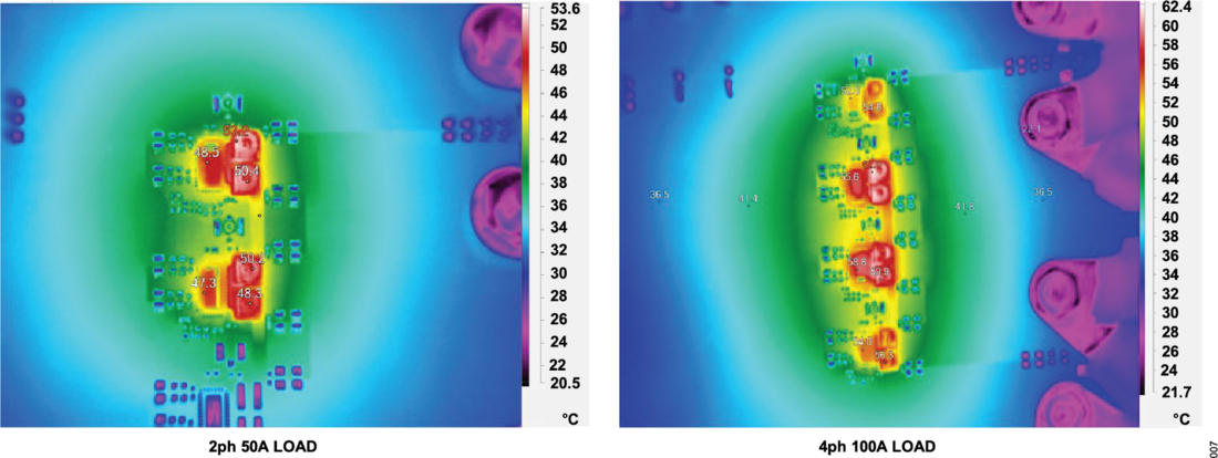
Thermal performance remains best-in-class across both configurations. As shown in Figure 8, measured at room temperature, the maximum device temperature in the 2-phase design is approximately 49 °C, while the 4-phase configuration reaches only 59 °C under full-load operation. These results highlight the LT7153SP’s excellent thermal scalability, making it well-suited for high-current, space-constrained optical-module power architectures.
Dynamic Output Voltage Control
Modern optical modules increasingly rely on dynamic voltage scaling to optimize performance and reduce overall power consumption. By adjusting the buck converter’s output voltage during system operation, the module can tune its internal core voltage in real time, enabling both performance scaling and energy savings.Method 1: Real-Time Voltage Adjustment Using DAC Control
Figure 9 illustrates a representative implementation in which the LT7153SP’s output voltage is dynamically programmed through a digital-to-analog converter (DAC) embedded in the optical module’s core logic. The DAC drives the VDAC pin, sourcing or sinking current at the feedback (FB) node. This injected current allows the LT7153SP to adjust VOUT to re-establish regulation.
Since the DAC modifies the FB node directly rather than altering the fixed internal reference, the converter can regulate to output voltages below the nominal reference voltage (0.4V for LT7153SPAV-0.4 or 0.5V for LT7153SP). This capability enables optical modules to implement fine-grained voltage scaling, supporting aggressive power-reduction modes and adaptive performance tuning.
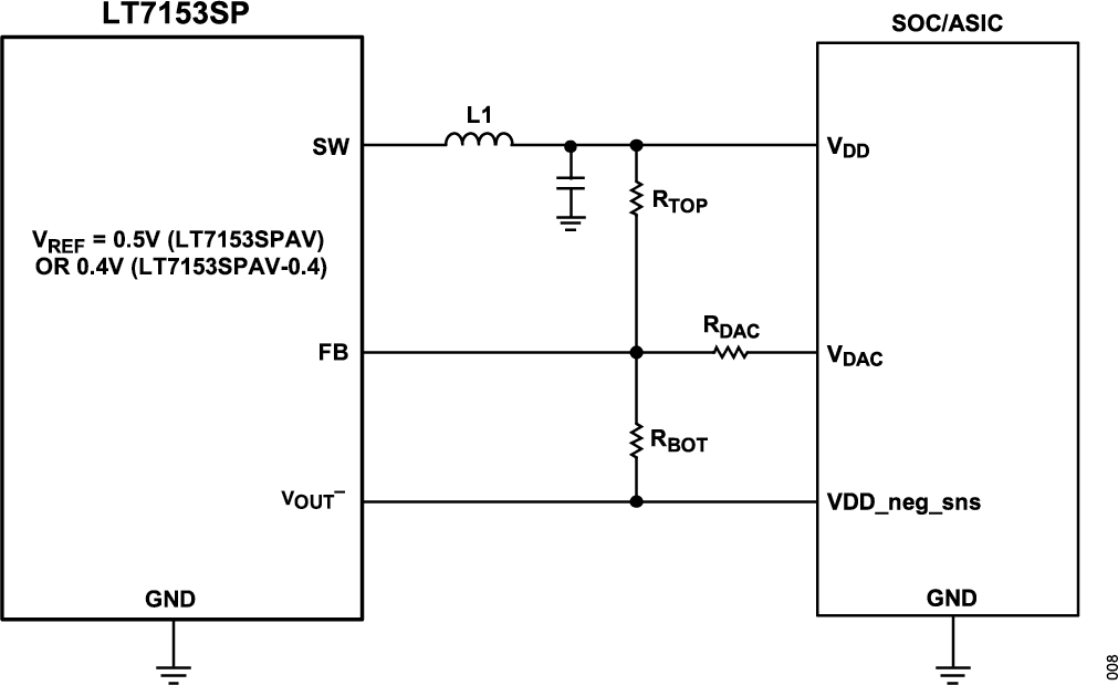
For most optical module ASICs, the required core supply voltage ranges from 0.4V to 1.0V. The resulting output voltage VDD delivered to the core can be expressed as the following equation:

Method 2: Output-Voltage Adjustment Using TRACK/SS Pin
An alternative method for output-voltage modulation uses the TRACK/SS pin. During startup, when the TRACK voltage is between 0V and VREF, it overrides the error amplifier's internal reference, causing the converter to regulate the output proportionally to the TRACK voltage. Once the TRACK pin rises above VREF, the tracking function is disabled, and the LT7153SP transitions to regulation based on its internal reference.
Although this method provides a simple way to command lower output voltages, it introduces two important limitations:
- Forced Continuous Mode (FCM) restriction: When the commanded output voltage is below the internal reference threshold (for example, 0.475 V for the LT7153SPAV), the device cannot operate in forced continuous mode (FCM). Many optical-module designs prefer FCM to maintain a consistent EMI profile, so this constraint may be unacceptable in noise-sensitive systems.
- Loss of tracking once FB exceeds VREF: After the feedback voltage rises above the internal reference, the TRACK/SS override is disabled. At that point, the converter cannot be commanded back to an output voltage below VREF using the TRACK pin alone. This limits the ability to perform dynamic voltage scaling after startup if the required voltage range crosses the VREF boundary.
These constraints make TRACK/SS useful primarily for controlled startup sequencing or for applications where the output remains below the reference voltage, while DAC-based control remains the preferred method for full dynamic voltage scaling.
PCB Design Guidelines
PCB layout is critical to the performance of a buck converter. Improper board layout can degrade performance, leading to increased EMI, voltage overshoot, instability, and lower efficiency. In high-frequency switching environments typical of buck converters, even small parasitic elements, such as trace inductance and capacitance, can cause substantial performance degradation. Additionally, component placement, trace routing, grounding strategy, and thermal management must be carefully considered. This section presents recommended PCB layout guidelines for the LT7153SP to help engineers achieve optimal electrical and thermal performance.
PGND and SGND
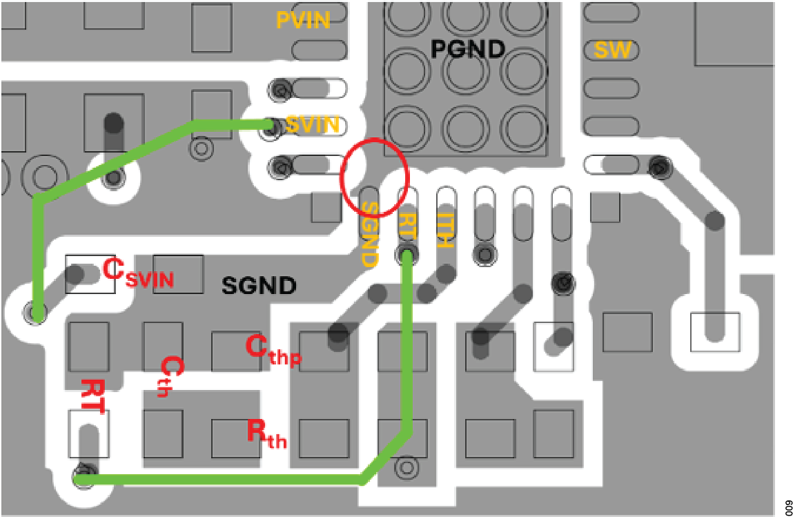
PGND, referred to as power ground, is the ground connection over which higher pulsed currents flow. SGND, known as Signal Ground, is the fundamental ground through which other signals pass and is typically very stable. In LT7153SP, the ground of some sensitive signals, such as ITH, RT, and SVIN, should be connected to an SGND. These signals are susceptible to noise and should be isolated from the GND that carries the return of switching currents.
The optimal connection between signal ground (SGND) and power ground (PGND) remains a widely discussed topic in PCB layout design. It is recommended for LT7153SP that the signal ground and power ground be connected together underneath the device through the SGND pin. In this way, the two ground voltage potentials are close to each other, and the device will be protected from disturbances. Figure 10 shows the EVAL-LT7153SP-AZ demo board connections as recommended.
RC Filtering of the Noise into the SVIN Pin
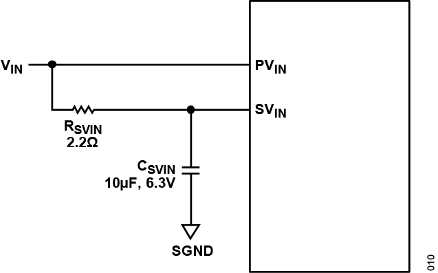
In the SVIN pin description of the LT7153SP datasheet, it is recommended to bypass the supply to the SVIN pin with a 10μF ceramic capacitor and a 2.2Ω series resistor. The SVIN pin powers the internal linear voltage regulator (LDO) and therefore requires a clean, filtered input supply. A low-pass filter is recommended between the input supply and the SVIN pin, as shown in Figure 11.
TRACK/SS Capacitor Connected to VOUT- instead of GND
TRACK/SS pin overrides the internal 0.5V reference, setting the feedback voltage to the TRACK/SS pin voltage. In this case, it servos the FB pin relative to VOUT- to this voltage. Place a capacitor between the TRACK/SS pin and the VOUT-pin instead of the GND pin.
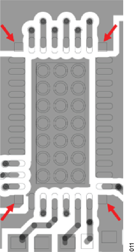
Four Corner Pins Connected to GND
The four corner pins are intended for mechanical support when the device is soldered to the PCB. Connect the four corner pins to GND as shown in Figure 12.
Dual-Phase (2xLT7153SP) Schematic Diagram
For optical module applications where loads demand more than 25A of current, multiple LT7153SP outputs can be tied together to run out of phase to provide more output current. Figure 8 in the LT7153SP datasheet shows the block diagram for connecting a dual-phase (2×LT7153SP) for a single 0.5V, 50A output running at a 2MHz switching frequency.
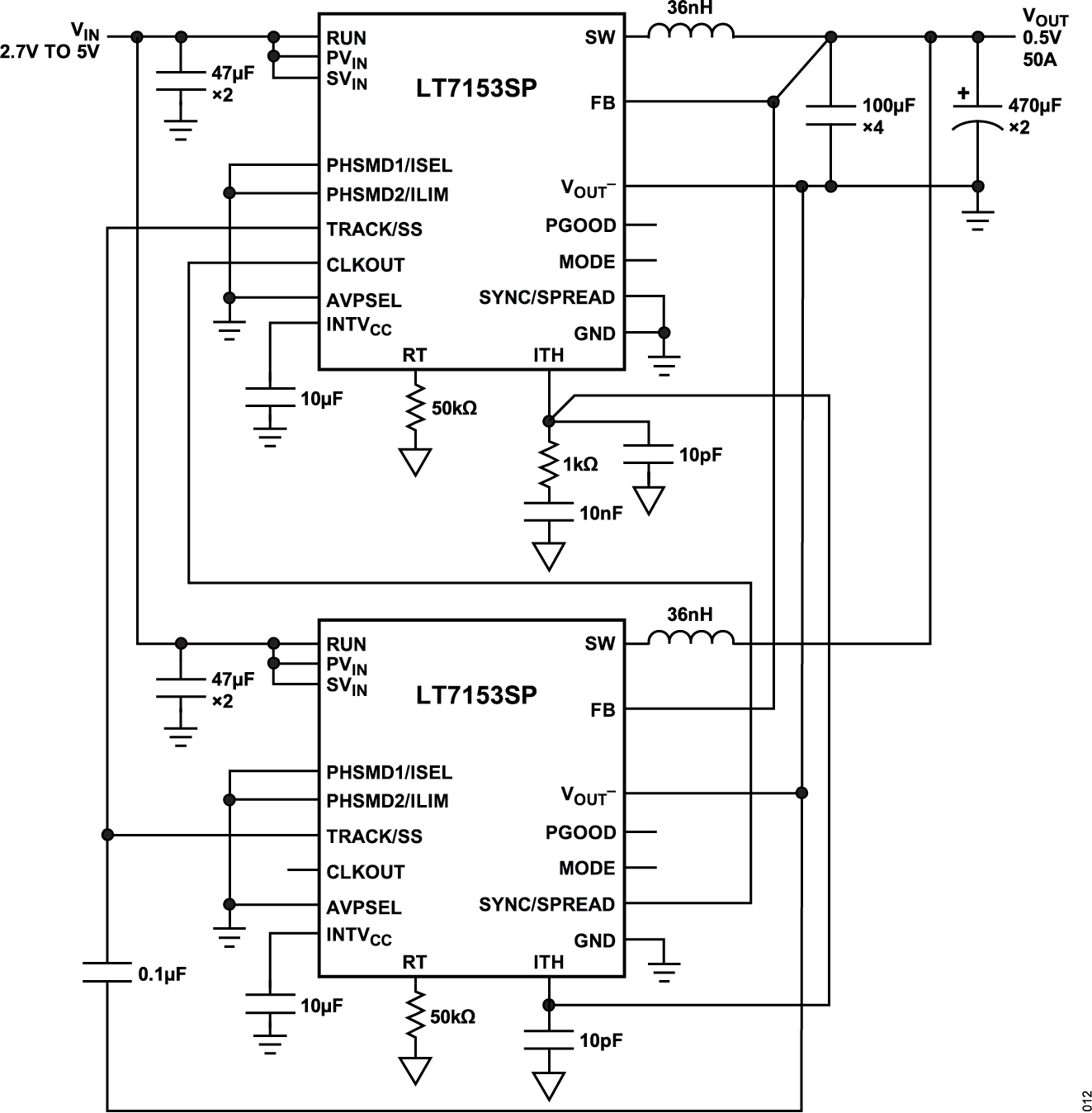
The following checkpoints should be reviewed when implementing the dual-phase connection:
- Connect the ITH pin, TACK/SS pin, FB pin, and VOUT- pin together, respectively, between the lead LT7153SP and the follower LT7153SP.
- Connect the lead’s CLKOUT pin to the follower’s SYNC/SPREAD pin
- Short both phase’s PHSMD1/ISEL and PHSMD2/ILIM to GND
With this connection, the lead LT7153SP and follower LT7153SP can achieve 180° out-of-phase interleaving. Refer to the Detailed configuration section in the LT7153SP datasheet for other phase counts.
For the layout recommendation, ensure that sensitive traces such as ITH, TRACK/SS, FB, VOUT-, SYNC, and CLKOUT are placed away from high-dv/dt traces, such as the switching node or input capacitor vias. Improper placement of these vias will interfere with the sensitive traces.
Conclusion
The LT7153SP is a 5V, ±25A monolithic step-down regulator designed for modern optical transceivers, emphasizing compact size, high efficiency, ultralow EMI, and fast transient response. It addresses the stringent requirements of next-generation optical modules, including power density, thermal management, and signal integrity.
作者