AN-2629: TMC9660 SPI Integration Guide
Interfacing the TMC9660 Using SPI
This application note describes how to integrate the TMC9660 API into an embedded host application and communicate with the TMC9660 through the host SPI interface. It covers device bring -up, addon loading to the TMC9660 RAM, persistent addon installation in external SPI flash memory, bootstrap configuration, transition to Parameter mode, basic motor operation, and advanced SPI communication techniques such as polling and pipelined access.
TMC9660 API
- Supports bootloader and Parameter mode
- MCU-independent and self -contained (no external dependencies)
- Code generation for configuration (UBLTools)
Required Hardware and Software
This guide uses the Raspberry Pi Pico as an example host controller for interfacing with the TMC9660. The following components and tools are required:
- TMC9660-STP -EVKIT or TMC9660-3PH-EVKIT
- Raspberry Pi Pico H (based on RP2040) and Raspberry Pi debug probe
- Jumper wires
- BLDC motor (e.g., QBL4208 -61-04-013-1k)
- Power supply (24V)
-
TMC9660 API (TMC-API)
- Available at https://github.com/analogdevicesinc/TMC-API
-
TMC9660 UBLTools, v1.2.0 or higher
- Available at www.analog.com/en/products/tmc9660.html
-
TMC9660 addon v1.0.0 or higher (.hex)
- Available at www.analog.com/en/products/tmc9660.html
Hardware Setup and Wiring
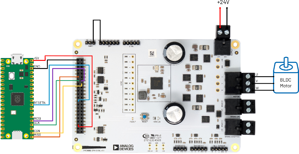
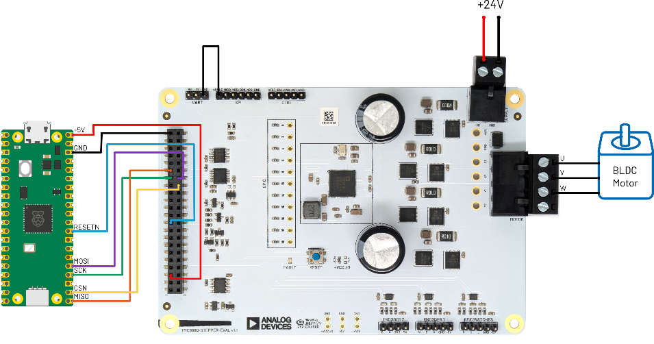
This guide uses the Raspberry Pi Pico as an example host controller for interfacing with the TMC9660. The interface wiring consists of seven jumper wires (see Table 1). Figure 1 and Figure 2 show the wiring diagram for the Raspberry Pi Pico and the supported evaluation boards. The wiring is the same for both the TMC9660 -3PH-EVAL and the TMC9660-STEPPER -EVAL. In addition to the supply voltage (+24V), the SPI lines are required for the initial bring-up. During bootloader operation, the TMC9660 requires an external VCCIO supply. In this example, the 5V supply from the Raspberry Pi Pico is connected to VCCIO. After the bootstrap configuration has been loaded, the TMC9660 may generate the required voltage internally depending on the selected configuration. The reset line is helpful during debugging.
Additionally the Pico debug probe is used to print serial messages to the terminal.
| Function | Raspberry Pi Pico | TMC9660-Stepper-Eval/TMC9660-3Ph-Eval |
| 24V | — | +VM |
| GND | — | GND |
| MISO | SPI0 RX (GP16) | SPI1_MISO (33) (J201) |
| MOSI | SPI0 TX (GP19) | SPI1_MOSI (32) (J201) |
| SCK | SPI0 SCK (GP18) | SPI1_SCK (31) (J201) |
| CSN | SPI0 CSn (GP17) | SPI1_CS (30) (J201) |
| GND | GND (38) | GND (43) (J201) |
| VCCIO (bootstrap 5V) | VBUS (40) | +5V_USB (5) (J201) |
| Reset | GP22 (29) | RESET_CTRL (19) (J201) |
| — | — | nHOLD ←→ GND |
SPI Flash Memory
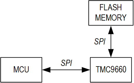
Optionally, an external SPI flash memory can be connected to the TMC9660 SPI1 interface using GPIO test points (TP). In this case, remove resistors R518, R523, R215, and R216 to bypass the existing circuit on the evaluation board. The required interface si gnals are listed in Table 2.
| Function | Raspberry Pi Pico | TMC9660-Stepper-Eval/TMC9660-3Ph-Eval | SPI Flash Memory |
| MOSI | — | GPIO18 (TP) | SPI MOSI |
| MISO | — | GPIO17 (TP) | SPI MISO |
| SCK | — | ENC1_N (TP) | SPI SCK |
| CSN | — | ENC2_A (TP) | SPI CSN |
| GND | GND (38) | GND (43) (J201) | GND |
| VCCIO (5V) | VBUS (40) | — | +5V |
Integrate the TMC9660 API
The TMC9660 API provides a convenient interface to the TMC9660, offering commands for both bootloader communication and Parameter mode.
This section describes how to integrate the TMC9660 API into the firmware project. To use the API, the callback functions must be implemented. For implementation examples, refer to theTMCL-C-Examples repository on GitHub.
- TMC9660-3PH-EVAL: TMC9660_3PH_EVAL_QBL
- TMC9660-STEPPER -EVAL: TMC9660_STEPPER_EVAL_QBL
Alternatively, create a new project from the Raspberry Pi Pico documentation and implement the SPI routine:
- Getting Started: https://pip-assets.raspberrypi.com/categories/610-raspberry-pi-pico/documents/RP-008276- DS-1-getting-started-with-pico.pdf?disposition=inline).
- SPI example: https://github.com/raspberrypi/pico-examples/blob/master/spi/mpu9250_spi/mpu9250_spi.c
To integrate the TMC9660 API into the project, follow these steps:
- Download the TMC9660 API.
- Include the TMC9660 API folder in the project.

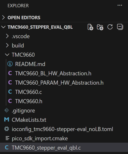
Figure 4. Include the TMC9660 API Files - Include the TMC9660 header.

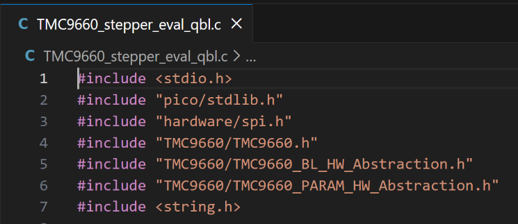
Figure 5. TMC9660 Header Files - Add TMC9660.c to the build configuration (CMakeLists).
-
Implement the following callback functions.
- tmc9660_getBusType()
- tmc9660_getBusAddresses()
- tmc_getMicrosecondTimestamp()
- tmc9660_readWriteSPI()
- tmc9660_readWriteUART()
- Send the first command tmc9660_bl_sendCommand() to test the communication.

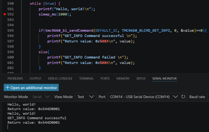
Figure 6. Reading the CHIP_TYPE Register through the Bootloader Interface
UART is not used in this example and tmc9660_readWriteUART()is included only as a placeholder. For further information, refer to the TMC9660 API readme file on GitHub (TMC-API/tmc/ic/TM9660).
The CHIP_TYPE return value is 0x544D0001 if the communication is successful. Make sure that the evaluation board is powered.
Install the Addon from MCU
Load the Addon to TMC9660 RAM
This section explains how to upload the SPI addon to the TMC9660 RAM from an MCU. The SPI addon is provided as a .hex file. The UBLTools code generator converts this .hex file into a C array, which is then copied to the firmware project. The TMC9660 API provides a command to load the addon array to the TMC9660.
-
Check the ublcli.exe version.
Start a new command prompt in the UBLTools folder.
Run: ublcli.exe --version
Response: ublcli.exe v1.2.0
-
Generate the addon array.
Run: ublcli.exe codegen addon TMC9660_addon_v1.0.0.hex
Result: The UBLTools generator creates the addon array and the tmc9660_bl_installAddon() function.

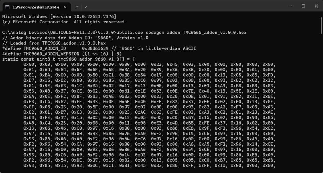
Figure 7. Addon Code Generation with ublcli.exe - Copy the addon array and the tmc9660_bl_installAddon() function to the project.
-
Upload and verify the addon.
Call the tmc9660_bl_installAddon_9660_v1_0 function to write the addon to the TMC9660. The addon version is indicated in the function name (here: “v1_0”). Read the addon ID and version (tmc9660_bl_getAddonInfo) to verify the addon upload.

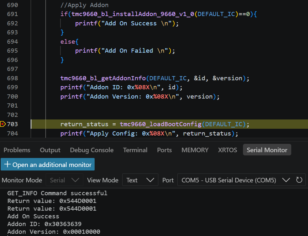
Figure 8. Read the Addon Version
Load the Bootstrap Configuration
Next, the bootstrap configuration is loaded into the TMC9660. The bootstrap configuration defines the hardware configuration of the TMC9660, including communication interfaces, pin assignments, motor driver configuration, and start-up behavior. In this gui de, the addon is loaded and the configuration is updated afterward. When using the TMCL-IDE and Landungsbruecke, the configuration is stored in a .toml configuration file, which is uploaded to the TMC9660 evaluation board. For the firmware project, UBLTool s generates the bootstrap configuration from the .toml configuration file. An evaluation board configuration file is used as the starting point. The configuration file is modified to use SPI instead of UART, which is the default setting for the Landungsbru ecke. Reference configuration files are available for the TMC9660 evaluation boards on GitHub (TMCL-C-Examples).
- TMC9660-3PH-EVAL: ioconfig_tmc9660-3ph-eval_noLB.toml
- TMC9660-STEPPER -EVAL: ioconfig_tmc9660-stepper-eval_noLB.toml
Using the .toml files, the bootstrap configuration C code is generated with the UBLTools and integrated into the firmware project. Finally, the TMC9660 API is used to load the configuration and enter Parameter mode .
-
Adapt the .toml file.
Update the .toml file to use the TMC9660 SPI0 interface as a communication interface instead of the SPI flash memory.
#### SPI Slave ###
[spi_slave]
enabled = true
spi_block = "SPI0"
pin_spi0_sck = 11

##### External memory #####
[spi_flash]
enabled = false
#spi_block    = "SPI0"   # "SPI0" or "SPI1"
#pin_cs       = 12       # 0-18
#frequency    = 10000000 # Hz
#pin_spi0_sck = 11       # 6, 11 (needed when spi_block = "SPI0")
Figure 9. Configuration Snippet for SPI Communication -
Generate the bootstrap configuration with the UBLTools.
Run: ublcli.exe codegen config --boot ioconfig_tmc9660-stepper-eval_noLB.toml
- Copy the bootstrap configuration code to the project.

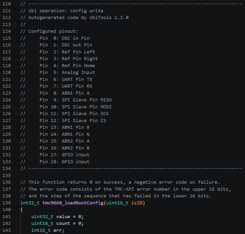
Figure 10. Bootstrap Configuration Code Generation -
Load the bootstrap configuration to the TMC9660.
To load the bootstrap configuration, call the API function tmc9660_loadBootConfig(). The function returns a status code of 0 if the upload completes successfully.

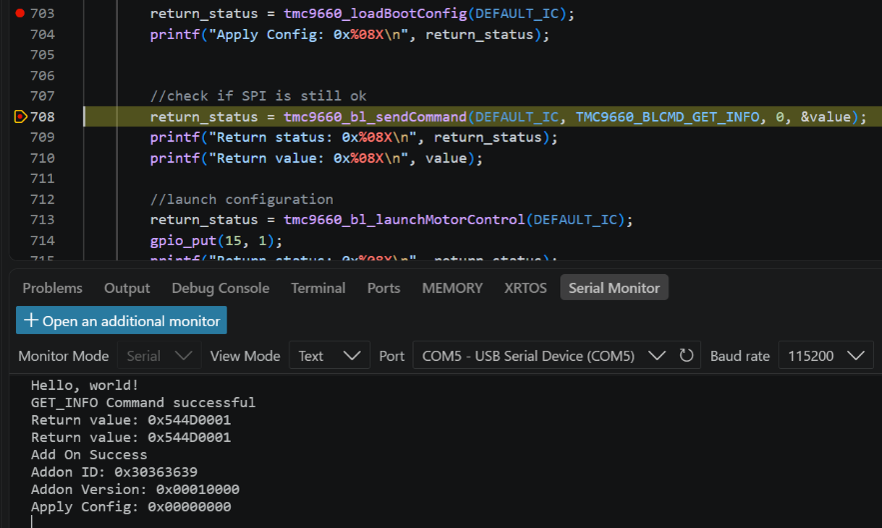
Figure 11. Uploading the Bootstrap Configuration -
Generate a start configuration code with the UBLTools.
Run: ublcli.exe codegen start
-
Copy the start configuration code to the project.

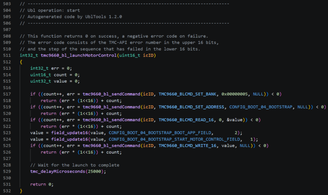
Figure 12. Start Configuration Function After launching motor control, the TMC9660 requires a short initialization period before parameter communication becomes available. The generated start function includes a delay of approximately 25ms. Alternatively, the FAULTN pin may be monitored to detec t when the Parameter mode becomes active.
Run: ublcli.exe codegen start (use the FAULTN pin)
For further details about this method, refer to the TMC9660 data sheet.
-
Start the configuration and enter Parameter mode.
Call the tmc9660_bl_launchMotorControl() function to enter the TMC9660 Parameter mode.


Figure 13. Enter Parameter Mode -
Verify the addon presence by reading the ID and version in Parameter mode.


Figure 14. Verify Addon ID and Version
Note: It is also possible to load the configuration before the addon. In this case, the no -boot option should be used, as otherwise the TMC9660 starts Parameter mode directly without the addon.
Install the Addon from SPI Flash Memory
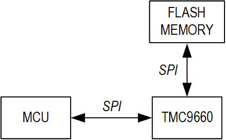
This section describes how to install the TMC9660 addon into external SPI flash memory from an embedded host MCU. The procedure is equivalent to the workflow used by UBLTools and consists of bootstrap configuration, erasing and writing the flash partition, programming the addon, writing the application header, starting the application, and verifying successful addon installation.
Load the Bootstrap Configuration
In this step, the bootstrap configuration is loaded into the TMC9660. The bootstrap configuration defines the hardware configuration of the TMC9660, including communication interfaces, pin assignments, motor driver configuration, and start -up behavior. Loa d the configuration with the SPI flash memory configuration before applying the addon. When using the TMCL -IDE and Landungsbruecke, the configuration is stored in a .toml configuration file which is uploaded to the TMC9660 evaluation board. For the firmwar e project, UBLTools generates the bootstrap configuration from the .toml configuration file. An evaluation board configuration file is used as a starting point. The configuration file is modified to use SPI instead of UART, which is the default setting for the Landungsbruecke. Additionally, the external SPI flash memory is configured. Reference configuration files are available for the TMC9660 evaluation boards on GitHub ( TMCL-C-Examples).
- TMC9660-3PH-EVAL: ioconfig_tmc9660-3ph-eval_noLB_SPIFlash.toml
- TMC9660-STEPPER -EVAL: ioconfig_tmc9660-stepper-eval_noLB_SPIFlash.toml
Using the .toml files, the bootstrap configuration C code is generated with the UBLTools and integrated into the firmware project. For the SPI flash memory addon installation, the bootstrap configuration should be loaded to configure SPI flash memory acces s, while the device remains in bootloader mode. Parameter mode should be entered only after the addon has been loaded and the application has been started.
-
Adapt the .toml file.
Update the .toml file to use the TMC9660 SPI0 interface for host communication interface and SPI1 for external flash memory:
#### SPI Slave ###
[spi_slave]
enabled = true
spi_block = "SPI0"
pin_spi0_sck = 11

##### External memory #####
[spi_flash]
enabled      = true
spi_block    = "SPI1"   # "SPI0" or "SPI1"
pin_cs       = 15       # 0-18
frequency    = 25000000 # Hz
#pin_spi0_sck = 11      # 6, 11 (needed when spi_block = "SPI0")
Figure 16. Configuration Snippet for SPI Communication and SPI Flash Memory
SPI1 uses the pins GPIO18 for MOSI, GPIO17 for MISO, ENC2_A/GPIO15 for CSN, and ENC1_N/GPIO14 for SCK (Table 2). Disable or reconfigure any conflicting pin functions in the configuration file.
-
Generate the bootstrap configuration with the UBLTools.
Run: ublcli.exe codegen config –boot ioconfig_tmc9660-stepper-eval_noLB_SPIFlash.toml
-
Copy the bootstrap configuration code to the project.

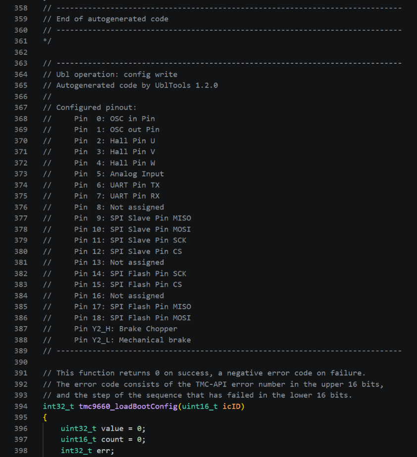
Figure 17. Bootstrap Configuration Code Generation -
Load the bootstrap configuration to the TMC9660.
To load the bootstrap configuration, call the UBLTools codegen function tmc9660_loadBootConfig(). The function returns a status code of 0 if the upload completes successfully.

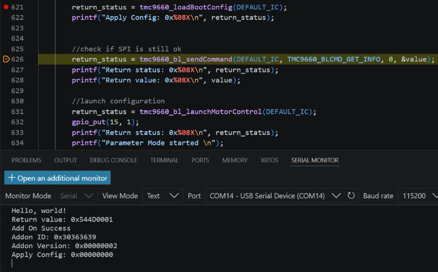
Figure 18. Uploading the Bootstrap Configuration -
Generate the start configuration code with UBLTools.
Run: ublcli.exe codegen start
-
Copy the start configuration code to the project.

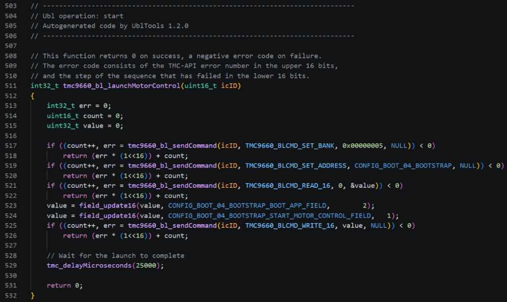
Figure 19. Start Configuration Function After launching the motor control, the TMC9660 requires a short initialization period before parameter communication becomes available. The generated start function includes a delay of approximately 25ms. Alternatively, the FAULTN pin may be monitored to d etect when Parameter mode becomes active.
Run: ublcli.exe codegen start (use the FAULTN pin)
For further details about this method, refer to the TMC9660 data sheet.
Erase the SPI Flash Memory
Before writing a new addon, the corresponding SPI flash memory must be erased. In this example, the whole chip is erased. It is also possible to erase only the partition sector. The host MCU first sends FLASH_SENDCMD (bootloader command 36) to enable flash memory write access and then sends the erase command through the bootloader.
| Command Order | Command | Example Value | Description |
| 1 | FLASH_SENDCMD | 0x00060000 | Enable write of SPI flash memory |
| 2 | FLASH_SENDCMD | 0x21000000 | Send 1 byte |
| 3 | FLASH_SENDCMD | 0x10000000 | Read out 3 bytes from the buffer |
| 4 | FLASH_SENDCMD | 0x00C70000 | Erase chip |
| 5 | FLASH_SENDCMD | 0x21000000 | Send 1 byte |
| 6 | FLASH_SENDCMD | 0x10000000 | Read out 3 bytes from the buffer |
| 7 | MEM_IS_BUSY | 0: not busy | Read SPI flash memory busy state |
Poll the SPI flash memory busy state with MEM_IS_BUSY (bootloader command 40) until MEM_IS_BUSY = 0 before starting the next flash memory operation. Refer to the TMC9660 data sheet for a detailed description of FLASH_SENDCMD and MEM_IS_BUSY.
Partition the SPI Flash Memory
This section describes how to partition the external SPI flash memory for use with the TMC9660 bootloader and addon. The partition table defines the location and size of all bootloader -managed data stored in the SPI flash memory and allows the TMC9660 bootloader to locate and load the addon applications during startup.
The TMC9660 bootloader expects a partition table at the beginning of the external SPI flash memory. During initialization, the bootloader reads this partition table to identify available partitions and determine the location of the addon.
A typical flash memory layout is shown in Table 4.
| Flash Memory Address | Name | Sector Size |
| 0x00000000 | Partition table | 0x00001000 |
| 0x00001000 | Settings (type = “TMCL_CONFIG”) | 0x00001000 |
| 0x00002000 | Script (type = “TMCL_SCRIPT”) | 0x00002000 |
| 0x00004000 | Addon (type = “APP”) | 0x00002000 |
In this example, the addon partition starts at address 0x00004000 and occupies 0x2000 bytes of SPI flash memory. The Settings and Script partition are omitted in the following example, and the address range 0x1000 –0x3FFF is unused.
Partition Table Structure
The partition table is located at flash memory address 0x00000000 and contains the partition header followed by partition entries, including the partition entry for the addon. The bootloader validates the partition table before attempting to access any par titions.
A partition table contains:
-
Partition header
- Partition table length
- Partition table CRC
- Magic number
- Flash memory information (size, sector)
-
Partition entry
- Name
- Type
- Offset
- Size
The following partition file (.toml) defines a single partition for the addon:
# Modified partition file for the TMC9660-STEPPER-EVAL and TMC9660-3PH-EVAL
# to support a stored addon
# These boards use a W25X40CLSNIG SPI Flash
# Partition for TMCL_CONFIG and TMCL_SCRIPT omitted

partition_config_version = "v1.0"

[part_table]
version = "v1.1"
size = 0x00080000 # Memory size: 4Mibit = 512KiB
sector_size = 0x1000 # Sector size: 4KiB

[[part_table.partition]]
name = "addon"
type = "APP"
offset = 0x4000
size = 0x20000
writable = true
The partition table information shown in the .toml file, flash memory layout overview, and bootloader command sequence represents the same data in different formats. During code generation, UBLTools converts the partition definition into the binary partiti on table structure expected by the TMC9660 bootloader. The generated partition table is then written to flash memory starting at address 0x00000000. The addon partition entry specifies an offset of 0x00004000 and a size of 0x00002000, which corresponds to the addon partition shown in the flash memory layout. During startup, the bootloader validates the partition table CRC, locates the APP partition, and uses the partition offset to locate the addon application.
To update the partition table from an MCU, write SET_BANK = 1 (bootloader command 9) to write to the external SPI flash memory. Set the memory address using SET_ADDRESS (bootloader command 11). Then WRITE_32_INC (bootloader command 19) writes the partition table entries and increments the address by 4 bytes for the next write access. Example commands are shown in Table 5.
| Command Order | Command | Offset [Bytes] | Example Value | Description |
| 1 | SET_BANK | — | 0x00000001 | Set memory bank to SPI |
| 2 | SET_ADDRESS | — | 0x00000000 | Set memory address |
| 3 | WRITE_32_INC | 0 | 0x00000028 | Write: Partition table size |
| 4 | WRITE_32_INC | 4 | 0xD08471BA | Write: CRC |
| 5 | WRITE_32_INC | 8 | 0x0101CAFE | Write: Magic number, major/minor version |
| 6 | WRITE_32_INC | 12 | 0x00000C13 | Write: Memory size index, memory sector index |
| 7 | WRITE_32_INC | 16 | 0x6F646461 “addon” | Write: Partition name |
| 8 | WRITE_32_INC | 20 | 0x0000006E “n” | Write: Partition name |
| 9 | WRITE_32_INC | 24 | 0x00000000 | Write: Partition name |
| 10 | WRITE_32_INC | 28 | 0x00000080 | Write: Partition type |
| 11 | WRITE_32_INC | 32 | 0x00004000 | Write: Partition offset |
| 12 | WRITE_32_INC | 36 | 0x00002000 | Write: Partition size |
The generated partition table must be consistent with the flash memory layout used by the bootloader. The values shown in the command sequence correspond to the generated partition table for flash memory containing a single partition for the addon. In the following example, only one partition entry is defined for the addon.
Partition table size = 16 + 24 x 𝑁𝑝𝑎𝑟𝑡𝑖𝑡𝑖𝑜𝑛𝑠 = 40 = 0x28
For the W25X40CL flash memory used on the evaluation boards, the configuration specifies a flash memory size of 0x00080000 bytes (512KiB) and a sector size of 0x1000 bytes (4KiB). These values are encoded into the header value 0x00000C13:
Flash memory size = 2 𝑠𝑖𝑧𝑒 𝑖𝑛𝑑𝑒𝑥 = 219 = 0x80000
Sector size = 2𝑠𝑖𝑧𝑒 𝑖𝑛𝑑𝑒𝑥 = 212 = 0x1000
Size index = 19 = 0x13
Sector index = 12 = 0x0C
The least significant byte contains the memory size index (0x13), and the next byte contains the sector size index (0x0C).
Refer to the TMC9660 data sheet for the calculation of the CRC. Different partition layouts result in different partition table contents, CRC values, and table sizes.
Create the Addon Array
This section explains how to create the addon array. The SPI addon is provided as a .hex file. The UBLTools code generator converts this .hex file into a C array, which is then copied to the firmware project.
-
Check the ublcli.exe version.
Start a new command prompt in UBLTools folder (changes to the environment variables are only effective in a new console).
Run: ublcli.exe --version
Response: ublcli.exe v1.2.0
-
Generate the addon array.
Run: ublcli.exe codegen addon TMC9660_addon_v1.0.0.hex
Result: The UBLTools generator creates the addon array and the tmc9660_bl_installAddon function

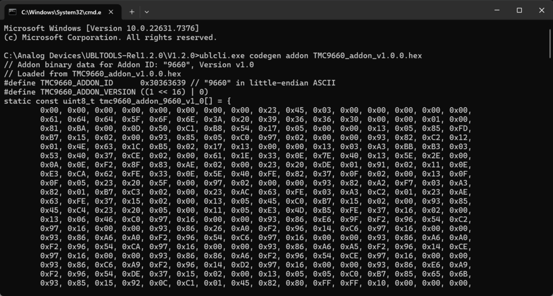
Figure 21. Addon Code Generation with ublcli.exe -
Copy the addon array and the tmc9660_bl_installAddon() function to the project.
Write the Addon to External SPI Flash Memory
The first 8 bytes of the generated addon array are reserved for the application header and are not transferred as part of the addon write procedure.
The example in this section installs the addon TMC9660_addon_v1.0.0.hex, with the addon ID 9660 and version v1.0.
Addon Array
The address 0x4008 is used because the first 8 bytes of the partition are reserved for the addon header consisting of the length and CRC fields.
| Command Order | Command | Example Value | Description |
| 1 | SET_BANK | 0x00000001 | Set memory bank to SPI |
| 2 | SET_ADDRESS | 0x00004008 | Set memory address |
| 3,4,… | Repeated WRITE_32_INC | Addon Data | Write addon data, 4 bytes at a time. |
Note: The bootloader automatically sends the Write Enable command to SPI flash memory (refer to the TMC9660 data sheet).
The MCU converts the addon byte array (generated from UBLTools) into little -endian 32-bit words and transfers the payload using repeated WRITE_32_INC commands.
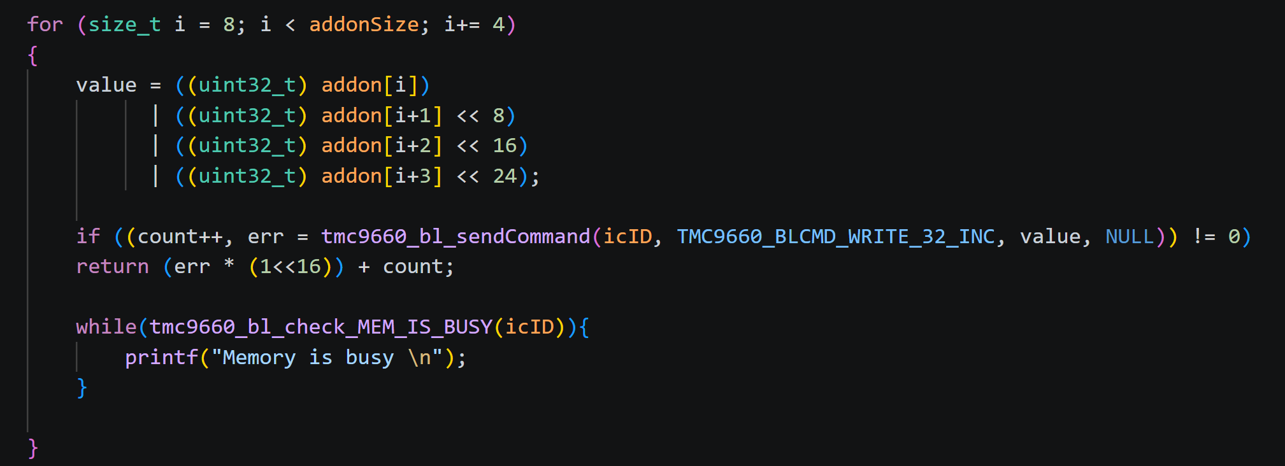
WRITE_32_INC writes a 32-bit value to the currently selected address and automatically increments the internal address pointer by four bytes after each write operation. The complete addon array is transferred sequentially until the entire addon has been pr ogrammed.
Application Header
After the addon array has been successfully programmed, the application header (consisting of the addon length and CRC) must be updated.
The length field is located at address 0x4000. The length value corresponds to the application size expected by the bootloader. Next, the CRC32 checksum is written using the dedicated bootloader command.
| Command Order | Command | Example Value | Description |
| 1 | SET_BANK | 0x00000001 | Set memory bank to SPI |
| 2 | SET_ADDRESS | 0x00004000 | Set memory address |
| 3 | WRITE_32_INC | 0x00000C00 | Write: Addon length |
| 4 | SET_ADDRESS | 0x00004000 | Set memory address |
| 5 | WRITE_CHECKSUM | 0x89B50AB5 | Write: CRC |
Note that WRITE_CHECKSUM starts at the selected application header address (0x4000 in this example).
After the checksum is written, the bootloader requires a short time to process it. For example, with an SPI frequency of 10MHz, a delay of approximately 10ms is required. This delay allows the bootloader to complete internal checksum processing before the application is started.
Load the Addon from External SPI Flash Memory to TMC9660
Once the addon array and application header have been written successfully to the flash memory, the addon can be loaded from SPI flash memory and started. There are three options for loading the addon from SPI flash memory.
Manual Application Launch
To manually launch an application, START_APP (bootloader command 27) must be called with the memory address pointing at the start of a present and valid application residing in the selected memory bank. The manual start sequence is shown in Table 8.
| Command Order | Command | Example Value | Description |
| 1 | SET_BANK | 0x00000001 | Set memory bank to SPI |
| 2 | SET_ADDRESS | 0x00004000 | Set memory address |
| 3 | START_APP | 0x00000000 | Start an application from the selected memory bank at the selected memory address. |
Then launch motor control and enter Parameter mode. Call the tmc9660_bl_launchMotorControl function to enter TMC9660 Parameter mode:

Update the Bootstrap Configuration
The configuration file can be configured to automatically load the addon from the SPI flash memory. Set load_spi_code to load from the external SPI memory to the TMC9660 RAM and run the addon application. Optionally, also set start_motor_control to load an d run the motor control system from the ROM application code. The relevant bootstrap settings are shown in Figure 24.
################################################################################
# Boot configuration for TMC9660-3PH-EVAL
################################################################################

io_config_version = "v1.0"

[app_settings]
app_type = "param"    # "param", "reg"

[bootstrap]
fault_on_config = true
load_spi_code = true
start_motor_control = true
Generate a new loadBootConfig function using the UBLTools code generator and integrate it into the project.
Store the Bootstrap Configuration in OTP
The bootstrap configuration can be permanently stored in TMC9660 OTP memory to automatically apply it on power-on. Three steps are required:
-
Identify an empty OTP page.
The OTP memory of the TMC9660 is organized into pages. To store a configuration, it can be programmed into one of the first four pages of the OTP with a page tag value of 4. Before programming a new configuration, it is recommended to verify that the targe t OTP page is unused. An empty OTP page can be identified by reading back the complete page content with OTP_LOAD (value = page number). If the command replies with OTP_ERROR (18), the page is empty. Because the highest valid OTP page is used first, the pages are checked in descending order. An example sequence for identifying an empty OTP page is shown in Table 9.
Table 9.Example Bootloader Command Sequence for OTP Page Identification Command Order Command Example Value Description 1 OTP_LOAD 0x00000003 Load an OTP page into the OTP memory bank. OTP_ERROR (0d18) Read: Status 2 OTP_LOAD 0x00000002 Load an OTP page into the OTP memory bank. OTP_ERROR (0d18) Read: Status 3 OTP_LOAD 0x00000001 Load an OTP page into the OTP memory bank. OTP_ERROR (0d18) Read: Status 4 OTP_LOAD 0x00000000 Load an OTP page into the OTP memory bank. OTP_ERROR (0d18) Read: Status Result: All pages are blank and can be written programmed.
For further details regarding OTP memory and configuration storage refer to the TMC9660 data sheet.
-
Write the OTP page buffer.
Write the bootstrap configuration to the OTP page buffer. Use the updated bootstrap configuration as reference. Set the memory bank to OTP (3) and the memory address to 0 to access the OTP page buffer. The OTP page buffer write sequence is shown in Table 10.
Note: All settings must be written, even if the default configuration is used.
In the bootstrap configuration (offset 8), the following parameters are relevant for the startup and addon installation from flash memory:
- START_MOTOR_CONTROL (bit 12) – Start the motor control based on the BOOT_MODE selection.
- START_SPI (bit 14) – Start code from the SPI flash memory.
Table 10.Example Bootloader Command Sequence Write OTP Page Buffer Command Order Command Offset Example Value Description 1 SET_BANK — 0x00000003 Set memory bank to OTP 2 SET_ADDRESS — 0x00000000 Set memory address 3 WRITE_16_INC 0 0x0000000B Write: BOOT_00_POWER/LDO configuration 4 WRITE_16_INC 2 0x0000FF01 Write: BOOT_01_ADDRESS/address 5 WRITE_16_INC 4 0x00000000 Write: BOOT_02_UART_TXEN_DELAY 6 WRITE_16_INC 6 0x00000780 Write: BOOT_03_BOOT_INTERFACE 7 WRITE_16_INC 8 0x00005202 Write: BOOT_04_BOOTSTRAP 8 WRITE_16_INC 10 0x0000F079 Write: BOOT_05_FLASH 9 WRITE_16_INC 12 0x00000000 Write: BOOT_06_EEPROM 10 WRITE_16_INC 14 0x00000000 Write: BOOT_07_GPIO_DATA_0_15_INIT 11 WRITE_16_INC 16 0x00000000 Write: BOOT_08_GPIO_DIR_0_15_INIT 12 WRITE_16_INC 18 0x0000FFC0 Write: BOOT_09_GPIO_PULLUP_0_15_INIT 13 WRITE_16_INC 20 0x00000003 Write: BOOT_0A_GPIO_PULLDOWN_0_15_INIT 14 WRITE_16_INC 22 0x00008E00 Write: BOOT_0B_GPIO_16_18_INIT 15 WRITE_32_INC 24 0x003D2663 Write: BOOT_CLK_SEL_INIT 16 SET_ADDRESS — 0x00000020 Set memory address 17 WRITE_16_INC 32 0x00000001 Write: BOOT_10_APP_CONFIG_0/ABN encoder, Hall 18 WRITE_16_INC 34 0x00000000 Write: BOOT_11_APP_CONFIG_1/ABN encoder, reference switches, step/dir 19 WRITE_16_INC 36 0x0000727E Write: BOOT_12_APP_CONFIG_2/mechanical brake, brake chopper, watchdog 20 WRITE_16_INC 38 0x00000000 Write: BOOT_13_APP_CONFIG_3/SPI encoder 21 WRITE_16_INC 40 0x00000005 Write: BOOT_14_APP_CONFIG_4/external memory storage -
Burn the OTP.
Follow the OTP burn procedure (refer to the TMC9660 data sheet, errata EDS -1):- Send SET_BANK, value 0.
- Send SET_ADDRESS, value 0x4801B010.
- Send READ_32.
- Clear bit 0 of the read value (0x00000001).
- Send WRITE_32, with the modified read value as a write value.
- Wait for the VDRV voltage to drop below 8.4V. The duration for this depends on the attached capacitor. With a 10μF capacitor, this takes 1.0s (typ).
- Send OTP_BURN.
- The request value selects which OTP page to burn with bits 7 -0 and what OTP page tag to write into the OTP page with bits 10 -8.
Configure and Operate the Motor in Open Loop
After the TMC9660 parameter communication has been verified, the device can be configured to run the motor. It is recommended to first perform the initial bring -up of the TMC9660-EVAL with the Landungsbruecke and TMCL -IDE to determine further configuration settings.
In the next steps, the tmc9660_param_sendCommand is used to configure the TMC9660 and run the motor:
-
Verify the parameter command API.
In TMC9660 Parameter mode, the Parameter mode API is used. To verify communication, call a GAP function using tmc9660_param_sendCommand.
-
Configure and operate the motor in open loop.
An example parameter sequence for open -loop operation with an BLDC is shown in Figure 25.
Write TMC9660_PARAM_MOTOR_TYPE = 3             //BLDC/PMSM motor
Write TMC9660_PARAM_MOTOR_POLE_PAIRS = 4       //Number of motor pole pairs
Write TMC9660_PARAM_OPENLOOP_VOLTAGE = 1000    //Open-loop voltage amplitude
Write TMC9660_PARAM_COMMUTATION_MODE = 3       //Open-loop commutation
Write TMC9660_PARAM_TARGET_VELOCITY = 10000    //Target electrical velocity
Figure 25. Example Command for Running Motor in Open Loop
The values shown in Figure 25 are intended as an example only. Actual motor parameters depend on the connected motor and power stage configuration.
SPI Communication Change Notes
Changes from the Data Sheet
This section describes the changes for the SPI communication applied by the addon. The reworked SPI function deviates slightly from the protocol described in the TMC9660 data sheet in the following ways:
-
Modified SPI reply:
- The first reply byte is now 0xAD for a response, 0x00 if no response is available.
- Replies to requests with checksum errors now also have a first byte of 0xAD. The checksum error is reported within the second byte (TMCL status) with a value of 1.
-
Added NOP command:
- Sending a request with operation = 0xFF does not cause any response to be sent. This is intended to be used as a way of retrieving a response without queuing another command. This is referred to as a “NOP command”.
-
Added support for pipeline communication:
- When retrieving a reply, a new request can be sent at the same time.
-
Modified behavior for short SPI transactions (<8 bytes):
- Any datagram with less than 8 bytes does not create a request —the TMC9660 ignores these. Reply data remains the same until a datagram of at least 8 bytes is sent.
Practical Usage – Polling
Any SPI transaction that is less than 8 bytes long does not count as a received request and does not take up a receive slot. Additionally, the data being sent back by the TMC9660 remains unchanged by such short transactions. Only a transaction of at least 8 bytes causes the reply data to be sent out in full, and subsequent accesses return “No response available” data (all zeroes).
Simple Access without Pipelining
Basic SPI operation of the TMC9660 consists of sending an 8 -byte command, polling with short datagrams until the reply is ready, and then reading out the reply by sending a NOP command:
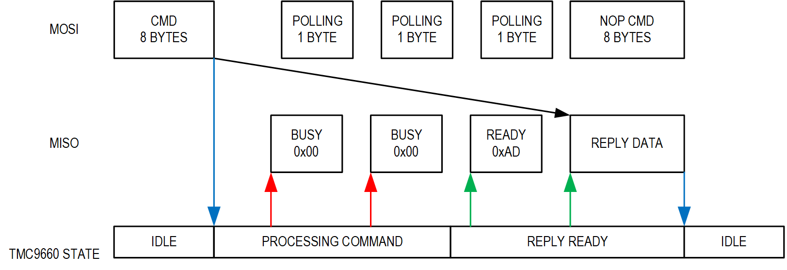
Note: Waiting for the reply instead of polling is possible; however, the internal processing times are variable and thus, a worst-case approach of waiting and then reading the reply would be significantly slower than a polling approach.
Doing repeated simple accesses then consists of repeating this sequence for every command.
Pipelined Access
Repeated simple access is not the fastest way to communicate with the TMC9660:
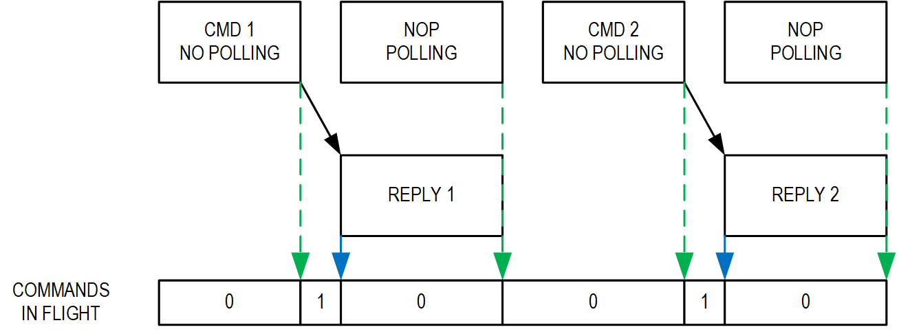
Note: “Polling” in a command box refers to performing single -byte polling until a reply is ready before sending the given command (Figure 27). Conversely, “No polling” refers to sending a command without this polling operation.
Instead, when sending multiple commands in a row, it is faster to use the sending command to retrieve the previous command’s reply:
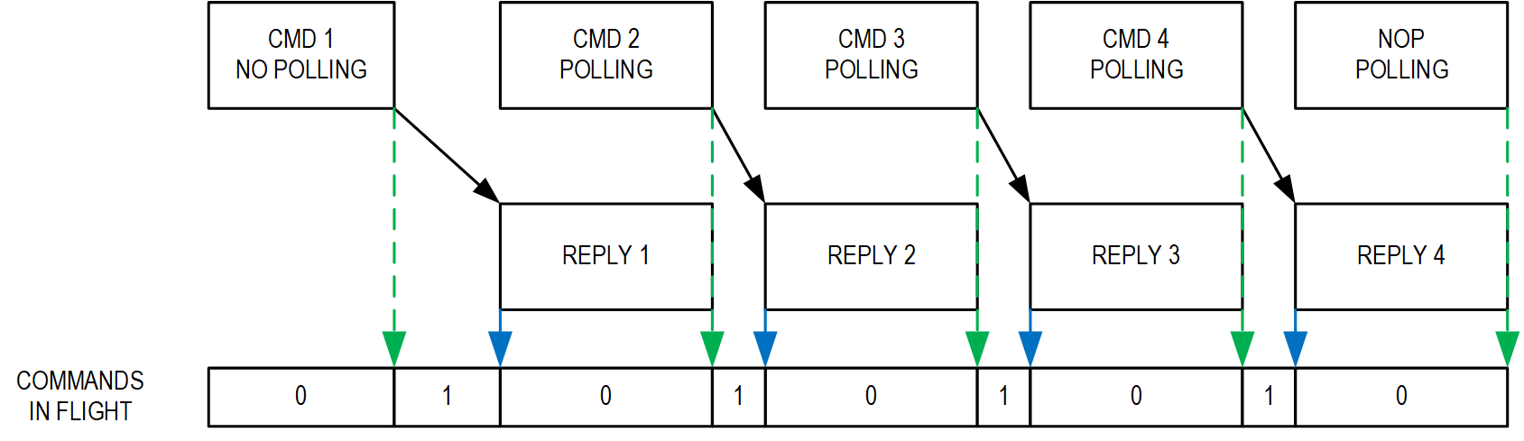
Here, the sending of subsequent commands overlaps with the retrieval of a previous command’s reply. Getting the final reply of such a sequence is then done with a NOP command.
TMC-API Reference Notes
To use the TMC9660 in C/C++ code, the TMC-API is available. This section details how to use the TMC -API for the SPI access methods (including pipelining functions) with the addon.
TMC-API SPI Functions
The TMC-API offers multiple basic functions to access the TMC9660 Parameter mode through SPI:
- A basic access function (tmc9660_param_sendCommand) for sending commands. When the API is configured for SPI operation (tmc9660_getBusType returning TMC9660_BUS_SPI), this function sends an SPI request followed by polling until it can receive the reply. This function is for basic access and is not the best choice for fast repeated access.
- A low-level access function (tmc9660_param_sendPipelinedSPICommand ) that allows implementation of the pipeline strategies detailed above. The following sections describe this function and show how to implement pipelining .
Understanding the Pipelined Access Function
The tmc9660_param_sendPipelinedSPICommand function has the following parameters:
- icID: This is the TMC-API’s way of allowing multichip implementations. All chip -specific functions of the TMC-API take this parameter, and all IC -level callback functions get called with this parameter. Based on it, the user application can perform functio ns such as identifying which physical bus peripheral to forward the TMC-API’s requests to.
Note: In all of the following code examples, the define DEFAULT_IC is passed for this. - cmd, type, index, requestValue: These values correspond to the request to send to the TMC9660. “cmd” refers to the “Operation” in the data sheet, “index” refers to the “Motor/Bank”, and “requestValue” refers to the “Data”. If only a reply is needed without a new request to be sent, cmd must be set to 0xFF.
- replyValue: This pointer is used to return a reply value to the application. It may be NULL if the reply value is not needed.
Note: Not every call of this function may have a reply value to hand back. - requireReply: This parameter controls whether the function expects a reply to come back alongside the request being sent. If set, it polls until a reply is ready (SPI status = 0xAD) and then sends the request alongside retrieving that reply.
- timeout_us: When requireReply is set, this parameter controls the timeout for how long polling is attempted. If this parameter is set to zero, the polling does not time out. If it is nonzero, the polling aborts after the specified number of microseconds ha s passed, and the TMC-API returns a timeout error.
Note: In all of the following code examples, the define SPI_TIMEOUT is passed for this. -
Return value (signed 32 bit):
- A negative value when a TMC-API-level error occurred (e.g., polling timeout)
- A TMCL status byte (1-255) when a reply was received
- A value of zero if no reply was received
Each call to this function sends a request (8 -byte SPI datagram) to the TMC9660. If “requireReply” is set, it first polls the TMC9660 by sending repeated 1-byte datagrams until the TMC9660 reports that a reply is available (first reply byte = 0xAD) or until timeout. If the TMC9660 replies with data, this function returns the TMCL reply status code (1 - 255) and stores the reply value in the “replyValue” pointer. Note that even if “requireReply” is not set, a reply may be available and is returned by the TMC -API if the access sequence was sufficiently slow.
Implementing the Pipelined Access with the TMC -API
To implement pipelined access with the TMC -API, perform the following sequence:
- Start the pipeline with a command without polling.
- Keep sending commands with polling.
- Send a final NOP command to retrieve the final reply.
In C code, this is accomplished as shown in Figure 29 (error handling of each TMC-API call is omitted for simplicity):
// Request 1: GET_INFO MODULE_ID
// This request is sent without polling
err = tmc9660_param_sendPipelinedSPICommand(
    DEFAULT_IC,
    157, 0, 0, 0, &replyValue,
    false, 0 // <- Polling disabled
);

// Request 2: GET_INFO VERSION
// This request is sent with polling
err = tmc9660_param_sendPipelinedSPICommand(
    DEFAULT_IC,
    157, 1, 0, 0, &replyValue,
    true, SPI_TIMEOUT // <- Polling enabled
);

// Reply received for GET_INFO MODULE_ID: 0x00000033

// Request 3: GET_VERSION HEX
// This request is sent with polling
err = tmc9660_param_sendPipelinedSPICommand(
    DEFAULT_IC,
    136, 1, 0, 0, &replyValue,
    true, SPI_TIMEOUT // <- Polling enabled
);
// Reply received for GET_INFO VERSION, 0x00010000

// Request 4: NOP command to retrieve the final reply
// This request is sent with polling
err = tmc9660_param_sendPipelinedSPICommand(
    DEFAULT_IC,
    0xFF, 0, 0, 0, &replyValue,
    true, SPI_TIMEOUT // <- Polling enabled
);
// Reply received for GET_VERSION HEX, 0x00330100
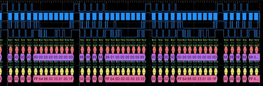
Each request is proceeded by a sequence of polling datagrams that only send a single byte. Each time the reply is 0x00, the datagram is aborted, and a new one is started. Once the reply is 0xAD, the rest of the datagram is transmitted. In the Figure 30screenshot, the first 8-byte datagram sends a GetInfo request (cmd = 0x9D). The second 8-byte datagram then contains the reply for that request, while another request for GetVersion (cmd = 0x88) is sent at the same time.