AN-2593: ADRV904x Transceiver VSWR
Scope
This application note assists in designing the ADRV904x voltage standing wave ratio (VSWR). The VSWR feature reports return loss at the antenna port and generates alarms based on predefined thresholds for return loss. The VSWR feature measures forward signal power and reflected signal power having maximum amplitude for the calculation of return loss.
The VSWR can be used to detect antenna or antenna cable faults. The VSWR feature is not designed to protect the power amplifiers.
| Abbreviation | Definition |
| VSWR | Voltage Standing Wave Ratio |
| RWD | Reverse Direction Power |
| FWD | Forward Direction power |
| DPD | Digital Pre-Distortion |
| CLGC | Closed Loop Gain Control |
| TDD | Time Division Duplex |
| FDD | Frequency Division Duplex |
| ORx | Observation Receiver |
| SPDT | Single-Pole, Double Throw Switch |
| RL | Return Loss |
| RAM | Random Access Memory |
| RCI | Radio Control Interface |
| DFE | Digital Front-end |
| SPI | Serial Peripheral Interface |
| GPIO | General Purpose Input/Output |
VSWR Introduction
VSWR refers to a feature used to monitor the transmission line termination quality at the antenna (to detect disconnections or bad cables). Poor termination of a transmission line (i.e., mismatched impedance) causes a reflected signal to travel in the reverse direction. This results in reduced efficiency as less power is delivered to the antenna. The reflected signal can also damage components such as power amplifiers.
The VSWR function utilizes forward and reverse (reflected power from antenna) power measurement of test RAM data. Forward power (Gf) is fed back to ORx from the forward coupler and reverse power (Gr) via the reverse coupler.
With the forward and reflected power, compute the forward-reflected ratio as:

The reflected power can be from multiple sources, like the cavity filter, antenna cable, or antenna. The VSWR feature measures the reflected power with maximum amplitude and uses that for return loss.
And then the VSWR can be computed as:

Note that VSWR is not reported directly by the API; only return loss is reported.
VSWR Hardware Requirements
To utilize the VSWR feature in the ADRV904x, both forward and reverse signals need to be sampled back to the ORx for power measurement. Note that the same ORx port is utilized for other DFE calibrations, such as DPD and CLGC. When VSWR is active, the DFE calibrations do not run.
Typically, two couplers and an SP2T switch are required to feedback forward and reverse power back to the ORx port for power measurement.
Figure 1 is an example circuit for reference, where two directional couplers are used to measure forward and reverse power.


Figure 1. EVB VSWR Hardware Requirement, Separate Forward and Reverse Coupler Used.
Note the Figure 1 does now show the 1:4 ORx control switch.
Customers can use a dual directional coupler instead of the coupler RWD. However, this is not recommended if using DPD, as any interference from the antenna port can couple back to the ORx path while running DPD and can impact DPD performance.
Figure 2 is an example to use the receive path from the circulator for the VSWR reverse measurement.


Figure 2. EVB VSWR Hardware Requirement, Reverse Path Taken From Isolator Port.
Instead of a second switch, a directional coupler can also be used.
In this setup, there is additional loss between the forward-coupled output to the ORx switch and the reverse path to the ORx switch. This variance can be included as an ORx gain offset parameter in the VSWR configuration.
Theory of Operation
The VSWR implementation in ADRV904x is based on correlated forward and reverse power measurements using the ORx path. A playback RAM is used to preload and transmit a playback waveform along with actual data. There are two modes: RCI mode and RCI-hybrid mode.
In RCI mode, the baseband processor (BBP) (field-programmable gate array (FPGA)) controls VSWR enable and FWD/RWD direction switch, and these controls are also sent to the GPIO. Therefore, the ARM processor knows when to run VSWR.
In RCI-hybrid mode, VSWR enable is not required as it is controlled by the scheduler. ORx mapping switch and VSWR switch direction are controlled by the ADRV904x, and GPIO needs to be assigned for both ORx mapping and VSWR direction switch control.
Multiple Reflections
Several factors can cause reflections and signal interference in the observed signal. Depending on where the coupler is placed, reflections can come from the cavity filter, antenna cable, or antenna. It is assumed that the interface of the cavity filter is good and provides a good return loss, for example, better than 14 dB. Therefore, the reflected power mostly comes from the antenna cable or antenna, indicating the condition of the antenna.
Coupler Directivity
Coupler directivity is the ratio between the input signal at the coupled port and the unwanted reflected signal at the coupled port. For the forward coupler, the directivity is from the output port. For the reverse coupler, the directivity is from the input port (the transmitted signal). Couplers directivity determines the maximum return loss that can be measured. The typical directivity of surface mount-couplers is between 20 dB to 25 dB, which means that the transmitter power can be observed during reverse power measurement at 20 dBc to 25 dBc level.
Switch Isolation
Switch isolation measures the power of the leaked signal from the dangling switch port. For example, when the the switch isolation in the circuit is 50 dB, it means that when ORx receives the forward signal, it also receives the reverse signal with 50 dB loss, and vice versa. The directivity of the coupler or the isolation of the isolator impacts the reverse power measurement more compared to switch isolation.
Reflection from Cavity Filter
The cavity filter also causes a reflection. It adds to the antenna reflection (in phase or out of phase).
Reflection from Antenna
The reflection from an antenna or antenna connector is what is of interest. The Analog Devices, Inc., ADRV904x VSWR relies on maximum peak reflected power.
Gain and Return Loss Calculation
Increasing the number of accumulations increases the Capture Power mdB (CorrPeak) values. This increases the accuracy of the gain reported but consume more time for VSWR execution.
The formula used to calculate forward gain is:

where txPower is the power in the playback waveform. This gives gain between the point where the playback waveform is injected and the ORx port. It does not depend on the input power of the modulated signal waveform from BPP (FPGA).
Formula used for return loss:

Acculumator Operation
The number of accumulation iterations controls how often the playback waveform is played in a loop. The capture buffers know the length of the playback waveform and accumulate the ORx data into a buffer of the same length. More accumulation iterations take longer but provide more accurate result.
If there are N iterations, the power of the playback waveform increases by N2, whereas the power of the user data remains the same and is not dependent on accumulation.


Figure 3. Accumulation Iterations.
Accumulation Iteration Power and Time
It is recommended to keep the input signal level at −14 dBFs or below. This is assuming a peak-to-average ratio (PAR) of 8 dB and headroom of 6 dB for DPD gain expansion.
The test RAM waveform is kept at a power level ~50 dBc below the actual waveform. The absolute level of the test RAM waveform is −64 dBFs.
For an accumulation iteration of 10,000, the power increase is 10log(100002) = 80 dB.
For an accumulation iteration of 80,000, the power increase is 10log(800002) = 98 dB
The time taken is sampling rate (at DPD HB1 Output) × accumulation iteration count.
For 122.88 MSPS sampling rate and 10,000 accumulation iteration, the time taken is =10000/122.88e6 = ~81.4 μsec.
VSWR Implementation
VSWR function measures forward and reverse power and reports back the antenna return loss. This is with the assumption that the highest amplitude reflection comes from the antenna or antenna cable. VSWR function detects the maximum reflected power and reports the return loss for that signal.
VSWR Test Ram Signal
VSWR power measurements are correlated power measurements based on a test signal injected from a test RAM. This signal is a low-power signal injected in the band as per the CDUC/CDDC configuration. The test RAM injection point is in between DPD HB1 and DPD HB2.


Figure 4. Test RAM Data Injection Point.
VSWR test RAM is generated based on the configured carriers to avoid unwanted emissions. Test RAM data is kept at −65 dBFS by default. This level is user-configurable.
For good EVM, typically keep the test ram data at −50 dBc from the actual transmitted signal.
The typical recommended input signal level from BBP is −14 dBFS (8 dB PAR and 6 dB for DPD gain expansion).
VSWR Test Ram Signal Generation
VSWR test RAM generation is part of the ACE GUI in future software releases. Currently, test RAM waveforms are generated using MATLAB code. Contact the ADI applications team for a test RAM waveform.
VSWR Accumulator
VSWR accumulator is an input field, the default recommended is 10,000. The more the accumulator there are, the greater the power measurement accuracy becomes, but the time taken to run VSWR increases. More details are available in the Theory of Operation section.
The power measurement reported by VSWR is accumulated power and there is a difference in power reported as per the accumulation number entered. Accumulated power readbacks (forward power and reverse power) cannot be used for absolute power measurement of the signal. When power measurements are used for return loss, the scaling is equally applied for forward and reverse power measurements and does not impact return loss value.
Return Loss Qualifying Threshold
The return loss qualifying threshold is an input field. The VSWR engine does not report VSWR if the calculated return loss value is below this value. The default is kept at 40 dB, which means it reports return loss for all practical cases.
VSWR Path Delay
The VSWR operates by performing cross-correlations at various delays of the playback waveform and an accumulated ORx capture. The peak correlation power is used to calculate the return loss value, and the delay at which the peak power was found is reported as path delay.
In other words, VSWR measures the delay between the injection point of the VSWR playback waveform and the ORx. The VSWR playback injection point is between the DPD HB1 and DPD HB2 filters.
The path delay reported by VSWR differs from that of DPD. A small difference in path delay does not impact VSWR, as correlated power measurements are used and the Tx RAM power remains constant.
For the forward path, it searches for a maximum correlation between 0 and 300 samples. For the reverse path, it searches for the maximum correlation between the forward delay and 700 samples.
The sample rate at the injection point and ORx sample rate must match, the Analog Devices VSWR can interpolate the playback signal by 2× during comparison with ORx capture data to allow for the difference between the rates at the VSWR injection point and ORx. This interpolation occurs only when pre-HB2 is enabled and post-HB1 is disabled. In other cases, it assumes the rate is the same.
Transmitter Attenuation Change Handling
When a transmitter attenuation change occurs (whether manually by the user or due to CLGC) during data capturing, it affects VSWR accuracy. Therefore, VSWR checks the transmitter attenuation values before and after capturing. When the attenuation has changed by more than 0.5 dB, the VSWR calculations do not proceed, and that iteration is exited. In this case, it reports a 0xE048u error code while trying to capture the VSWR statistics.
This is not expected to be a common occurrence as typically CLGC is configured to make updates of 0.1 dB or 0.2 dB step size.
VSWR Accuracy
VSWR reports return loss with an accuracy of ±1 dB up to 20 dB.
VSWR can be calibrated during research and development (R&D) as shown in Figure 5 in the GUI section. The offset can be adjusted in the reverse path gain (reversePathOffsetmdB) field. This can improve the accuracy further.


Figure 5. Tx-ORx Mapping for 3-Pin Mode.
Note that this is with signal at −14 dBFs, test RAM data at −64 dBFs, and ORx power at −14 dBFs.
Different Modes For Tx-ORx Mapping and VSWR
These are the following modes for Tx-ORx mapping:
- RCI mode
- DFE mode (RCI-hybrid mode)
RCI Mode
In RCI mode, for FDD systems Tx-ORx mapping is controlled via SPI, while VSWR forward-reverse switching is managed via GPIO (VSWR direction).
For the TDD system, Tx-ORx mapping needs to be controlled by GPIO. Apart from the GPIO required for ORx switching, two additional GPIOs are required for VSWR: one for VSWR enable and one for VSWR direction.
VSWR enable/disable GPIO needs to be assigned via JSON. VSWR direction GPIO can be selected from the digital GPIO mapping under stream in ACE GUI.
Tx to ORx Mapping and VSWR Direction Set
Tx-ORx mapping is controlled by the stream processor. This invokes the streams required to set up a transmitter to ORx mapping configuration, and also sets the direction of the VSWR capture. VSWR direction can be set using Pin mode or API mode.
For Tx-ORx mapping, external switches are required as the ADRV904x has 8 transmitter channels and only two ORx channels. Tx0−Tx3 needs to be mapped to ORx0, and Tx4−Tx7 needs to be mapped to ORx1. Tx-ORx mapping can be defined in API mode or Pin mode.
In API mode, the Tx-ORx mapping and direction can be set using adi_adrv904x_TxToOrxMappingAndVswrDirSet() API.
The user can readback the Tx-ORx mapping and direction using adi_adrv904x_TxToOrxMappingAndVswrDirGet() API.
In Pin mode, GPIOs from FPGA are used for switch control and to inform the ADRV904x on which transmitter channel is connected to which ORx by giving the same signal via ADRV904x GPIO. In this mode, VSWR enable is part of the Tx-ORx mapping configuration. The VSWR direction uses separate GPIO assigned from the stream settings — digital GPIO mapping in ACE GUI. There is an option to use common VSWR direction using a single GPIO or separate GPIOs for the direction of ORx0 and ORx1.
Three aspects of stream processor configuration need to be input to generate the proper stream binary for a desired transmitter to ORx mapping. In these modes, the GPIO input pins send a signal to the stream processor which indicates the mapping to the ARM processor, and may properly run the calibrations. These are:
- Tx Observability: The user must configure a Tx Observability attribute for each transmitter channel. This defines which ORx channel a specific transmitter channel can be observed by. A single transmitter channel can only be observable to one ORxchannel. It is invalid for any Tx to be observed by both ORx0 and ORx1.
- GPIO Mapping Mode: For modes featuring fewer pins, there are additional constraints upon the user in terms of the configuration of the feedback path. The available modes are:
- 2-pin mode
- 3-pin mode
- 4 pin mode
- 6-pin mode
- 8-pin mode
- GPIOs for Tx to ORx Mapping: The user must define which GPIO pins are used to indicate the Tx to ORx mapping. Any of the 24 digital GPIO pins can be used to indicate the mapping Bits D0, D1, D2 up to D8 as per pin mode selected.
2-Pin Mode
In this mode, ORx1 and ORx2 share the same control from BBP.
The two GPIOs in a 2-pin mode need to be connected to the two SP4T switches and back to the assigned ADRV904x GPIO pins as shown in Figure 5.
The mapping in Table 2 is an example. The user needs to do mapping according to the SP4T connection and pin logic.
Users can change the below mapping from the pin table under stream settings in ACE GUI. For example, for D0 = 0 and D1 = 0, the user can connect Tx1 for DPD by changing the pin table or by changing directly in JSON.
| D1 | D0 | Enum | Mapping for ORx0 | Mapping for ORx1 |
| 0 | 0 | 0x0 | Tx0 - DPD | Tx4 - DPD |
| 0 | 1 | 0x1 | Tx1 - DPD | Tx5 - DPD |
| 1 | 0 | 0x2 | Tx2 - DPD | Tx6 - DPD |
| 1 | 1 | 0x3 | Tx3 - DPD | Tx7 - DPD |
3-Pin Mode
The 3-pin mode extends the 2-pin mode by adding a third GPIO pin to indicate VSWR enable. In 3-pin mode, Bits D0, D1, and D2 are used. D0 and D1 pin usage is similar to that in 2-pin mode, while the third pin, D2, is used for VSWR enable. Once VSWR is enabled, no other DFE tracking calibrations run.
Table 3 explains the ORx mapping in 3-pin mode.
| D2 | D1 | D0 | Enum for ORX0 | ENUM for ORX1 | Mapping for ORx0 | Mapping for ORx1 |
| 0 | 0 | 0 | 0x0 | 0x4 | Tx0 - DPD | Tx4 - DPD |
| 0 | 0 | 1 | 0x1 | 0x5 | Tx1 - DPD | Tx5 - DPD |
| 0 | 1 | 0 | 0x2 | 0x6 | Tx2 − DPD | Tx6 − DPD |
| 0 | 1 | 1 | 0x3 | 0x7 | Tx3 - DPD | Tx7 - DPD |
| 1 | 0 | 0 | 0x8 | 0xC | Tx0 - VSWR | Tx4 - VSWR |
| 1 | 0 | 1 | 0x9 | 0xD | Tx1 - VSWWR | Tx5 - VSWR |
| 1 | 1 | 0 | 0xA | 0xE | Tx2 - VSWR | Tx6 - VSWR |
| 1 | 1 | 1 | 0xB | 0xF | Tx2 - VSWR | Tx7 - VSWR |
4-Pin Mode
In 4-pin mode, ORx0 and ORx1 can be controlled independently. The D2 bit is used for VSWR enable and the D3 bit decides which ORx to be enabled.
| D3 | D2 | D1 | D0 | Enum for ORx0 | Enum for ORX1 | Mapping for ORx01 | Mapping for ORx11 |
| 0 | 0 | 0 | 0 | 0x0 | - | Tx0 - DPD | N/A |
| 0 | 0 | 0 | 1 | 0x1 | - | Tx1 - DPD | N/A |
| 0 | 0 | 1 | 0 | 0x2 | - | Tx2 - DPD | N/A |
| 0 | 0 | 1 | 1 | 0x3 | - | Tx3 - DPD | N/A |
| 0 | 1 | 0 | 0 | 0x8 | - | Tx0 - VSWR | N/A |
| 0 | 1 | 0 | 1 | 0x9 | - | Tx1 - VSWR | N/A |
| 0 | 1 | 1 | 0 | 0xA | - | Tx2 - VSWR | N/A |
| 0 | 1 | 1 | 1 | 0xB | - | Tx3 - VSWR | N/A |
| 1 | 0 | 0 | 0 | - | 0x4 | N/A | Tx4 - DPD |
| 1 | 0 | 0 | 1 | - | 0x5 | N/A | Tx5 - DPD |
| 1 | 0 | 1 | 0 | - | 0x6 | N/A | Tx6 - DPD |
| 1 | 0 | 1 | 1 | - | 0x7 | N/A | Tx7 - DPD |
| 1 | 1 | 0 | 0 | - | 0xC | N/A | Tx4 - VSWR |
| 1 | 1 | 0 | 1 | - | 0xD | N/A | Tx5 - VSWR |
| 1 | 1 | 1 | 0 | - | 0xE | N/A | Tx6 - VSWR |
| 1 | 1 | 1 | 1 | - | 0xF | N/A | Tx7 - VSWR |
| 1 N/A means not applicable. | |||||||
6-Pin Mode
The 6-pin mode is an extension of the 3-pin mode. Bits D0 to D2 control ORx0, and Bits D3 to D5 are used for ORx1. Bit D0 to D1 and Bits D3 to D4 are used for transmitter select, and Bits D2 and D5 are used for VSWR enable.
| D5 | D4 | D3 | D2 | D1 | D0 | Enum | Mappping for ORx01 | Mapping for ORx11 |
| - | - | - | 0 | 0 | 0 | 0x0 | Tx0 - DPD | N/A |
| - | - | - | 0 | 0 | 1 | 0x1 | Tx1 - DPD | N/A |
| - | - | - | 0 | 1 | 0 | 0x2 | Tx2 - DPD | N/A |
| - | - | - | 0 | 1 | 1 | 0x3 | Tx3 - DPD | N/A |
| - | - | - | 1 | 0 | 0 | 0x8 | Tx0 - VSWR | N/A |
| - | - | - | 1 | 0 | 1 | 0x9 | Tx1 - VSWR | N/A |
| - | - | - | 1 | 1 | 0 | 0xA | Tx2 - VSWR | N/A |
| - | - | - | 1 | 1 | 1 | 0xB | Tx3 - VSWR | N/A |
| 0 | 0 | 0 | - | - | - | 0x4 | N/A | Tx4 - DPD |
| 0 | 0 | 1 | - | - | - | 0x5 | N/A | Tx45 - DPD |
| 0 | 1 | 0 | - | - | - | 0x6 | N/A | Tx6 - DPD |
| 0 | 1 | 1 | - | - | - | 0x7 | N/A | Tx7 - DPD |
| 1 | 0 | 0 | - | - | - | 0xC | N/A | Tx4 - VSWR |
| 1 | 0 | 1 | - | - | - | 0xD | N/A | Tx5 - VSWR |
| 1 | 1 | 0 | - | - | - | 0xE | N/A | Tx6 - VSWR |
| 1 | 1 | 1 | - | - | - | 0xE | N/A | Tx7 - VSWR |
| 1 N/A means not applicable. | ||||||||
8-Pin Mode
The 8-pin mode is the same as the 3-pin with independent control for ORx0 and ORx1.
Bits D0 to D1 and Bits D4 to D5 are used for transmitter selection. Bits D2 and D6 are used for ORx selection independently. Bits D3 and D7 are used for VSWR enable or DFE calibrations independently.
| D7 | D6 | D5 | D4 | D3 | D2 | D1 | D0 | Enum | Mapping for ORx01 | Mapping for ORx11 |
| - | - | - | - | 0 | 0 | 0 | 0 | 0x0 | Tx0 - PDP | N/A |
| - | - | - | - | 0 | 0 | 0 | 1 | 0x1 | Tx1 - PDP | N/A |
| - | - | - | - | 0 | 0 | 1 | 0 | 0x | Tx2 - PDP | N/A |
| - | - | - | - | 0 | 0 | 1 | 1 | 0x3 | Tx3 - PDP | N/A |
| 0 | 1 | 0 | 0 | - | - | - | - | 0x4 | N/A | Tx4 - PDP |
| 0 | 1 | 0 | 1 | - | - | - | - | 0x5 | N/A | Tx5 - PDP |
| 0 | 1 | 1 | 0 | - | - | - | - | 0x6 | N/A | Tx6 - PDP |
| 0 | 1 | 1 | 1 | - | - | - | - | 0x7 | N/A | Tx7 - PDP |
| - | - | - | - | 1 | 0 | 0 | 0 | 0x8 | Tx0 - VSWR | N/A |
| - | - | - | - | 1 | 0 | 0 | 1 | 0x9 | Tx1 - VSWR | N/A |
| - | - | - | - | 1 | 0 | 1 | 0 | 0xA | Tx2 - VWSR | N/A |
| - | - | - | - | 1 | 0 | 1 | 1 | 0xB | Tx3 - VSWR | N/A |
| 1 | 1 | 0 | 0 | - | - | - | - | 0xC | N/A | Tx4 - VSWR |
| 1 | 1 | 0 | 1 | - | - | - | - | 0xD | N/A | Tx5 - VSWR |
| 1 | 1 | 1 | 0 | - | - | - | - | 0xE | N/A | Tx6 - VSWR |
| 1 | 1 | 1 | 1 | - | - | - | - | F | N/A | Tx7 - VSWR |
| 1 N/A means not applicable. | ||||||||||
DFE Mode (RCI-Hybrid Mode)
In RCI-hybrid mode or DFE mode, the VSWR enable is not required because the scheduler handles the VSWR calibration. The ORx switch control and the control signal for forward-reverse switch control are generated from the ADRV904x. The user needs to route preassigned GPIO for switch controls.
In DFE mode, the user can only support up to 5 GPIOs per ORX channel. GPIOs can be assigned based on the required bit configuration for customer hardware (SP4T and SP2T switches).
The user can select the GPIOs in the 24-bit digital GPIO pin selection and the 16 analog GPIO pin selection.
Refer to the enums section in the adrv904x_radioctrl_types.h from the software package for more details. See DFE Mode (RCIHybrid Mode).
Figure 7 is an example of how 68 to 70 for a GPIO are assigned in the JSON when the DFE ORX common bits are assigned.


Figure 6. GPIOs Enum.


Figure 7. GPIOs Assignment in the JSON.
In AUTO mode, the mapping and the direction are configured in the ADRV904x through GUI stream settings or JSON update. The GPIOs assigned in stream settings are utilized to control the external switches. This ensures that both ADRV904x and the switch are synchronized for the same mapping and FWD/RWD direction.
The transmitter to Orx mapping mode must be selected as DFE control mode (enum 32 in JSON) as "TxToOrxMappingMode": 32.
Figure 8 is an example of hardware configuration where 2 bits (Bits D0 and D1) are used for Tx-ORx mapping and is routed to the SP4T switch, while Bit D3 is used for VSWR reverse direction. By default, the direction bit must be in the forward direction.


Figure 8. Tx-ORx Mapping, VSWR — DFE Mode.
Figure 9 is the ACE GUI example of transmitter to Orx mapping mode and GPIO mapping details in the stream settings for AUTO mode.


Figure 9. Tx-ORx Mapping Mode and GPIO Mapping.
Table 7 represents the physical mapping for the example use case shown in the Figure 9.
| VSWR Direction | SP4T Control | ORx0 Mapping | ORx0 Mapping | |
| D2 | D1 | D0 | ||
| 1 | 0 | 0 | Tx0 – DPD/VSWR FWD | Tx4 – DPD/VSWR FWD |
| 1 | 0 | 1 | Tx1 – DPD/VSWR FWD | Tx5 – DPD/VSWR FWD |
| 1 | 1 | 0 | Tx2 – DPD/VSWR FWD | Tx6 – DPD/VSWR FWD |
| 1 | 1 | 1 | Tx3 – DPD/VSWR FWD | Tx7 – DPD/VSWR FWD |
| 0 | 0 | 0 | Tx0 – VSWR REV | Tx4 – VSWR REV |
| 0 | 0 | 1 | Tx1 – VSWR REV | Tx5 – VSWR REV |
| 0 | 1 | 0 | Tx2 – VSWR REV | Tx6 – VSWR REV |
| 0 | 1 | 1 | Tx3 – VSWR REV | Tx7 – VSWR REV |
This is mapped to meet the example hardware requirement of Figure 8. Users can customize the pin table in ACE GUI based on the external circuitry. When separate controls are required for ORx0 and ORx1, the user must use DFE ORx Bit 0 to 2 for ORx0 and Bits 4 to 6 for ORx1. (Note that this is just an example, any GPIO can be selected.)
API Functions
VSWR Enable
The user can enable or disable the VSWR tracking calibration using the adi_adrv904x_DfeTrackingCalsEnableSet( ) API.
The channel mask has to be set as TX_VSWR_MASK for enabling/disabling VSWR.
adi_adrv904x_DfeTrackingCalsEnable►
Set(adi_adrv904x_Device_t* const, const
uint32_t calMask, const uint32_t
channelMask, const adi_adrv904x_DfeApp►
TrackingCalEnableDisable_t enableDisableFlag);
VSWR Test Ram Waveform Load
The user can write the VSWR pulse RAM waveform using adi_adrv904x_VswrPlaybackDataWrite() API.
The playback waveform data has real and imaginary data in tabbed format and contains a maximum of 1023 samples.
This data set is added to the signal on the data path after the Pre-DPD HB1 block.
adi_adrv904x_VswrPlaybackData►
Write(adi_adrv904x_Device_t* const
device, const uint32_t
txChannelMask, const adi_adrv904x_VswrPlay►
backData_t* const playbackData)
The user can readback the VSWR pulse RAM using VswrPlaybackDataRead() API.
adi_adrv904x_VswrPlaybackData►
Read(adi_adrv904x_Device_t* const
device, const uint32_t txChannelSel,
adi_adrv904x_VswrPlaybackData_t* const play►
backData);
VSWR Direction Set
VSWR direction can be set using pin mode or API mode.
- For pin mode, JSON needs to be modified for transmitter forward/reverse control GPIO along with Tx-ORx mapping.
- For API mode, the TxToOrxMappingAndVswrDirSet() API can be used to set the transmitter to ORX mapping and VSWR direction.
adi_adrv904x_TxToOrxMappingAndVswrDirGet() API can be used to read back the transmitter to ORX mapping and VSWR direction.
VSWR Configuration
The VSWR tracking configuration can be set using the VswrTrackingConfigSet() API. The user can set the number of accumulations in a capture, set the upper threshold for reported reflections, and configure minor and major alarms.
- adi_adrv904x_DfeAppCalVswrAlarmCfg
- int32_t thresholdmdB
- uint8_t iterWindow
- uint8_t iterThresholdCount
- adi_adrv904x_DfeAppCalVswrCfg
- uint32_t accumNumIter
- int32_t returnLossThreshmdB
- int32_t reversePathOffsetmdB
- adi_adrv904x_DfeAppCalVswrAlarmCfg_t minorAlarm
- adi_adrv904x_DfeAppCalVswrAlarmCfg_t majorAlarm
- VSWR reset: Reset the VSWR for required channels using the VswrReset() API.
VSWR Status
The user can read the VSWR status of a selected channel using the VswrStatusGet() API. The user can read the average forward and reverse powers, reflection coefficients such as return loss, sample delay, fractional delay, timestamps for the forward and reverse captures, and transmitter playback waveform powers, etc.
Few Guidelines
Minimum and maximum values of configurable parameters are as follows:
- VSWR_MAX_ACCUM_ITERATIONS = 0x3FFFFFU;
- VSWR_MAX_ALARM_ITER_WINDOW = 64U;
- minorAlarm.iterWindow, "Minor alarm iteration window cannot be larger than 64U");
- minorAlarm.iterThresholdCount, "Minor alarm threshold iter count cannot be larger than iter window size");
- minorAlarm.thresholdmdB, "Minor alarm threshold cannot be larger than returnLossThreshmdB");
VSWR Alarms and GP_INT
Alarms are set using VswrTrackingConfigSet() API based on the return loss measured. There is an option to generate two alarms, a minor alarm and a major alarm based on predefined return loss thresholds.
For example, when the minor alarm threshold is set to 10 dB and the major alarm threshold is set to 6 dB, a minor alarm is reported when the return loss calculated is less than 10 dB for X counts in Y iterations. X and Y are pre-programmed iteration counts.
Similarly, when the reported return loss is less than 6 dB, a major alarm is reported.
When alarms are generated, the software also reports this via corresponding error code.
The error code for minor alarm is 0xE04B and for major alarm is 0xE04C.
GP_INT can be raised using bit D45 of the upper GP_INT word. When that occurs, the BBIC has to use API functions to determine the cause (as there can be multiple sources for raising that bit) and to identify which channel (and potentially which reflection) the alarm refers to.
Errors and Error Codes
The VSWR errors and error codes can be found in adrv904x_dfe_app_error_tables.h from the source file package.
Testing VSWR with Ace GUI
This is the general sequence to test VSWR feature:
- Program with respective UC whether it is API mode/Pin mode/ RCI-hybrid mode.
- Enable the Tx and ORx channels (without data).
- Configure the VSWR Config parameters.
- Load the playback waveform for the channel for testing the VSWR.
- Run the VSWR tracking calibrations.
- Control the RF switch in VSWR forward and reverse directions.
- One update needs the direction to be switched in FWD and REV within 4 sec.
- Read the VSWR tracking status and statistics in FWD and REV directions. After the user gets REV statistics, the update count and the statistics must be reflected.
Initial Setup Requirement
Tx-ORx must be connected via an RF switch to allow switching between forward and reverse paths. Figure 10 is what the VSWR GUI looks like.


Figure 10. VSWR GUI.
There are three modes in which the user can test the VSWR:
- API mode
- Pin mode
- DFE control mode/AUTO mode
API Mode
In API mode, the transmitter to ORx mapping and the direction are set by using API. Based on the mapping and the direction, the external switch must be controlled using GPIOs from the FPGA.
Figure 11 illustrates the setup diagram.


Figure 11. Test Setup for API Mode.
Procedure to Test VSWR Feature in API Mode
The following test procedure describes testing the VSWR feature in the API Mode:
- Program the Usecase with Tx-ORx mapping state as shown in Figure 5.
- Enable the Tx and ORx channels
- Enter the VSWR Config parameters, such as the return loss qualifying threshold, accumulation iterations, and major and minor alarm thresholds, as per testing, and select Set Config. The VSWR GUI provides a test option by programming the thresholds. See Figure 12.
Figure 13 shows the maximum and minimum ranges for all the VSWR Config parameters.

Figure 12. VSWR Default Threshold.


Figure 13. VSWR Config Range.
- Upload the playback data waveform.
- Select the particular Tx channel mask which is needed to test the VSWR feature.
- Load test RAM data waveform. Test RAM data can be generated from ACE GUI (TBD) or can be loaded as a file.
- Select Upload Playback data from a file to upload a pregenerated test RAM waveform.
- Enable VSWR.
- Control the RF switch in VSWR forward and reverse directions during API mode. The switch needs to be toggled within 4 seconds for 1 update to take place. The user can use the VSWR Direction section in GUI to reverse the direction of the switch with a single button Cycle Direction and Apply. See Figure 14.


Figure 14. VSWR Direction Configuration.
- Check the VSWR tracking status and statistics.
- After the forward and reverse switching occurs, the user can read the VSWR tracking status and statistics, as shown for the second and third iterations.
The iteration and update count increment, and the percent complete shows 100%.
From the statistics, the user can report the forward and reverse powers in mdB, return loss, sample delay, fractional delay, forward path gain, reverse time stamp, and forward time stamp. See Figure 15.

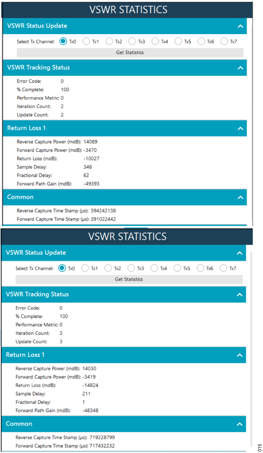
Figure 15. VSWR Statistics.


Pin Mode
In Pin mode, the mapping and direction are set using the assigned GPIO pins and are driven by the FPGA. The same GPIO pins that are connected to the ADRV904x are also connected to the external switch. This is recommended for TDD mode where precise timing is crucial.
Block Diagram
Tx to ORx mapping mode and GPIO mapping details in the stream settings are configured for pin mode:


Figure 16. Test Setup Example for Pin Mode.


Figure 17. GPIO Mapping Details for 8-Pin Mode.


Figure 18. Stream Settings — Tx-ORx Mapping Example.
Procedure to Test VSWR Feature in Pin Mode
The following test procedure describes testing of the VSWR feature in the Pin Mode:
- Program the Usecase with GPIO mapping details
- Enable the Tx and ORx channels.
- Enter the VSWR Config parameters, such as return loss qualifying threshold, accumulation iterations, major and minor alarm thresholds, as per testing requirements, and select Set Config. The VSWR GUI provides a test option by programming the thresholds.
- Upload the playback data waveform.
- Select the specific Tx channel mask for testing the VSWR feature.
- Load test RAM data waveform. Test RAM data can be generated from ACE GUI (TBD) or can be loaded as a file.
- Select Upload Playback data from a file to upload a pregenerated test RAM waveform.
- Set the direction and the output for the forward direction using GpioOutputDirSet() API and GpioWrite() API respectively.
- Read the VSWR status and statistics using the VswrStatusGet() API.
- Set the direction and output for reverse direction using GpioOutputDirSet() API and GpioWrite() API, respectively.
- Read the VSWR status and statistics using the VswrStatusGet() API. The user must be able to read the return loss, reverse power, forward power, and minor and major alarm counts.
AUTO Mode/DFE Control Mode
In AUTO mode, the mapping and the direction are set in the ADRV904x and are available on assigned GPIOs. These GPIOs are used to control the external switches so both the ADRV904x and switch are aligned for the same mapping and FWD/REV direction.
Tx to ORx mapping mode and GPIO mapping details in the stream settings are configured for AUTO mode:


Figure 19. Tx-ORx Mapping DFE Mode and GPIO Mapping.
Block Diagram


Figure 20. Test Setup Example for AUTO Mode.
Procedure to Test VSWR Feature in AUTO Mode
The following test procedure describes testing the VSWR feature in AUTO Mode:
- Program the Usecase with the mapping as shown in the Figure 19.
- Enable the Tx and ORx channels.
- Enter the VSWR Config parameters, such as return loss, qualifying threshold, accumulation iterations, major and minor alarm thresholds, as per the testing, and select Set Config. The VSWR GUI provides a test option by programming the thresholds.
- Upload the playback data waveform.
- Select the particular transmitter channel mask for testing the VSWR feature.
- Load test RAM data waveform. Test RAM data can be generated from ACE GUI (TBD) or can be loaded as a file.
- Select Upload Playback data from a file to upload a pregenerated test RAM waveform.
- Disable the tracking calibrations.
- Set the Tx to ORx mapping to forward direction using DfeCtrlTxToOrxMappingAndVswrDirSet() API.
- Enable VSWR tracking calibration using DfeTrackingCalsEnableSet() API.
- Read the VSWR status and statistics using the VswrStatusGet() API.
- Set the Tx to ORx mapping to reverse direction using DfeCtrlTxToOrxMappingAndVswrDirSet() API.
- Read the VSWR status and statistics using the VswrStatusGet() API. The user must be able to read the return loss, reverse power, forward power, and minor and major alarm counts.