AN-1523: 利用AD8368可变增益放大器扩展ADL5513对数检波器的动态范围
电路功能与优势
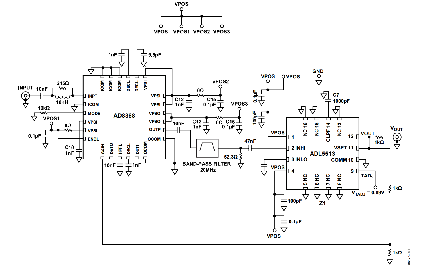
图1所示电路提供一种提高ADL5513对数检波器动态范围的 解决方案。为了实现这一目的,在ADL5513的输入端添加 一个AD8368可变增益放大器(VGA)。ADL5513的输出电压(VOUT)信号经过衰减,反馈到AD8368的增益控制输入,从而 对ADL5513输入端的功率进行精确控制。这种方法可将电 路的动态范围提高到95 dB,并且具有温度稳定性(见图 2)。输出电压与输入信号呈线性dB关系。


电路描述
通过添加一个单独的VGA(其增益控制输入直接来自VOUT),可以扩展ADL5513对数检波器的动态范围。此配置根据VGA增益控制范围扩展动态范围。为使整体测量保持线性dB,VGA必须提供线性dB(指数)增益控制功能。VGA增益必须随其增益偏置的增加而下降,下降方式与ADL5513相同。或者,可以使用具有适当电平转换功能的反相运算放大器。选择只需单个5.0 V电源且能够产生单端输出的VGA会很方便。AD8368满足所有这些条件。图1为原理示意图。使用AD8368的反向增益模式(MODE引脚为低电平),对于1.0 V的增益电压(VGAIN),增益以37.5 mV/dB的斜率下降至-12 dB。AD8368所需的电压VGAIN为ADL5513 输出的50%。为了调整该电压,需要在ADL5513的输出端插入一个分压器。在ADL5513输出的1.5 V范围内,AD8368的增益变化幅度为(0.5 × 1.5 V) ÷ (37.5 mV/dB) = 20 dB。此增益变化与ADL5513的75 dB增益范围(120 MHz时)相结合,使得AD8368输入端发生95 dB的变化时,VOUT发生1.5 V 的变化。
由于AD8368会放大带外噪声,因此AD8368和ADL5513之间使用一个带通滤波器来提高弱信号灵敏度。VGA会放大低功率信号并衰减高功率信号,使其适合ADL5513的可检测范围。如果使用具有更高增益和更低噪声系数的放大器,则可以实现大于90 dB的灵敏度,从而适用于接收信号强度指示器(RSSI)应用。
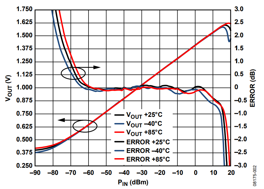
图2显示了120 MHz时扩展动态范围的数据结果以及相应的VOUT误差。
由于涉及高频率和宽动态范围,该电路必须构建在多层印刷电路板(PCB)上,其中至少有一层用于接地层。每个IC输入电源引脚必须通过0.1 µF低电感陶瓷电容去耦,如图1所示。对于极高频率,有些电源引脚具有额外的较小值去耦电容(低有效串联电感)。原理图上的0 Ω电阻代表可选的小值电阻(< 10 Ω)或铁氧体磁珠,添加这些元件可以增强去耦。
有关EVAL-ADL5513和EVAL-AD8368评估板的理想布局,请参考ADL5513和AD8368数据手册。
ADL5513和AD8368芯片级封装的底部有裸露焊盘。这些焊盘与芯片接地内部相连。将这些焊盘焊接至PCB的低阻抗接地层可确保达到额定的电气性能,并可提供散热功能。建议利用过孔将焊盘下方所有层上的接地层拼接在一起,以降低热阻抗。
常见变化
通过选择适当的带通滤波器,可以修改本应用笔记所述的应用电路,使其适用于AD8368和ADL5513工作范围内的任何中频(IF)。对于800 MHz以上的操作,可以用ADL5330代替AD8368。ADL5330 VGA可在10 MHz至3 GHz的频率下使用。使用ADL5330时,ADL5330 GAIN引脚和ADL5513增益控制电压之间需要一个反相器。在此应用中,可配置AD8061单电源运算放大器来用作反相器。