AN-1252: How to Configure the AD5933/AD5934 test update
Introduction
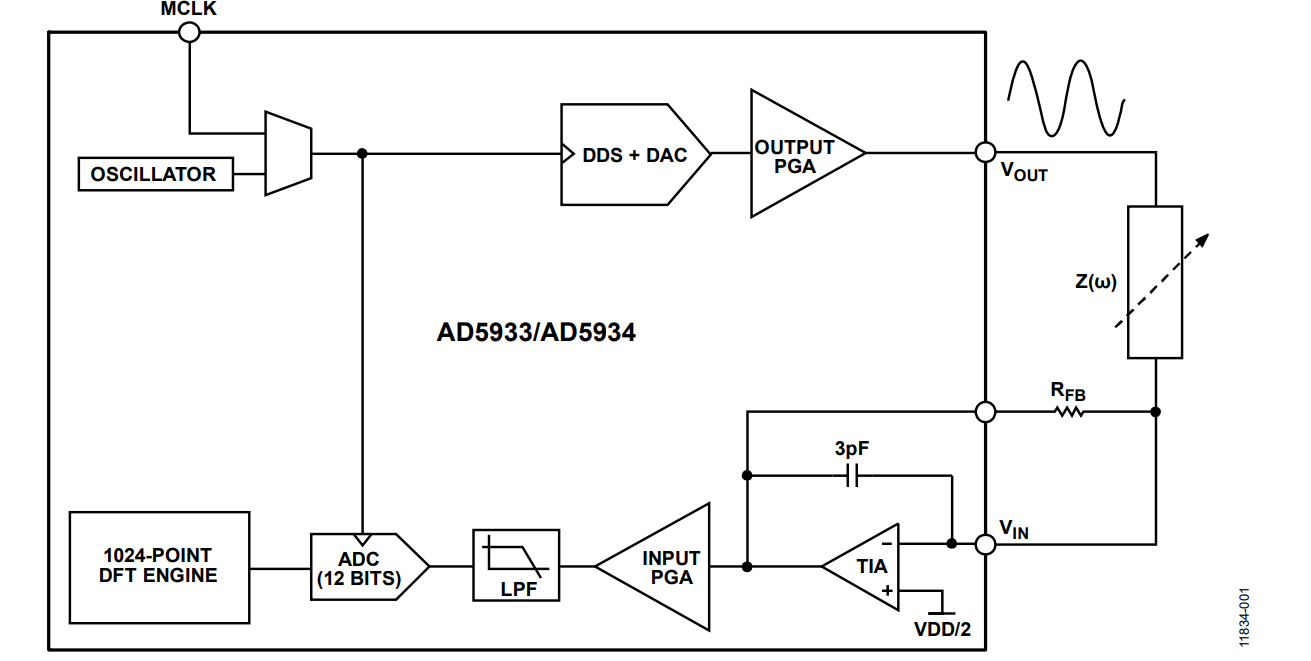
The AD5933 and AD5934 are high precision impedance converter system solutions. The main difference between these two solutions is the maximum measurable frequency. This application note applies to both parts. The main blocks of the AD5933 and AD5934 are shown in Figure 1.

The impedance converter is a finite system and has some limitations. This application note only aims to explain the optimum setup for measurements.
Impedance Measurement Blocks
Impedance converters can be divided into three different blocks: a transmit stage, a receive stage, and a discrete Fourier transform (DFT) engine.
Transmit Stage
The DDS core and the high speed DAC generate a sine wave signal used to excite the impedance.
The output programmable gain amplifier (PGA) is used for conditioning the output signal. It can be configured in four user selectable excitation voltages.
Receive Stage
The receive stage consists of:
- The transimpedance amplifier (TIA) that converts the current that crosses the impedance into voltage
- The input PGA that amplifies the TIA signal ×1 or ×5
- The ADC that samples the signal and fills the internal buffer (1024 points)
DFT Engine
Getting Started
Benefits of Adding an External AFE
CN-217 describes an external analog front end (AFE) designed to improve measurements.
This AFE has two main benefits: to reduce the output impedance of the signal source and to rebias the excitation voltage signal.
Rebiasing the DC Level
When connecting the impedance between VIN and VOUT, as shown in Figure 2, notice that the dc bias voltage is slightly different in the transmit stage and receive stage.

Figure 2. AD5933 Without External AFE.
The receiver dc offset is set to the ADC midscale, noninverting pin of the TIA, VDD/2, while the dc offset in the transmitter depends on the selected output voltage shown in Table 1.
| Range No. | DC Offset Voltage | V p-p |
| 1 | 1.48 | 1.98 |
| 2 | 0.76 | 0.97 |
| 3 | 0.31 | 0.383 |
| 4 | 0.173 | 0.173 |
An example of the different dc bias voltages is shown Figure 3 for Range 1 where VDD = 5 V

Figure 3. Excitation Output Voltage Without AFE.
Due to this mismatch, the dc level difference is amplified by the RFB, or, in other words, the ADC dynamic range is reduced.
Additionally, a dc voltage across a sensor can polarize it and/or degrade it over the sensor lifetime.
Reducing the Output Impedance
The internal output impedance depends on the amplitude voltage range selected and this may be as high as 2.4 kΩ. Therefore, since impedance cannot be considered negligible, it needs to be added into the equation. Typical values are shown in Table 2.
| Range No. | Typical Output Impedance, ZOUT |
| 1 to 4 (Adding external op amp) | >100 Ω |
| 1 | 200 Ω |
| 2 | 2.4 kΩ |
| 3 | 1 kΩ |
| 4 | 600 Ω |
The total measurable impedance is the unknown impedance and the system output impedance. To measure small impedances, adding the system output impedance may dramatically increase the range thus increasing the total measurable impedance. Consequently, this reduces the output current. To compensate, the value of RFB needs to increase. In other words, a high RFB value means worse SNR and lower sensitivity in your system.
Implementing these suggestions is relatively easy. Rebiasing the dc level is straightforward; just add a high-pass filter. If you are planning to design the high-pass filter, refer to AN-581 Application Note, Biasing and Decoupling Op Amps in Single Supply Applications.
To reduce the output impedance and have the ability to measure low impedances, the recommended op amp of choice is the AD8606 (ZOUT = 1 Ω). You may consider the AD8602 as a lower cost alternative. Figure 4 shows the AFE implementation in the EVAL-AD5933EBZ, Rev. C1.
The second AD8606 is used as a TIA due to the lower leakage and noise; the internal receive stage TIA is operating as a voltage follower.

Figure 4. AD5933 with AFE.
Configuring the Part
Correctly configuring the AD5933/AD5934 is key to getting the most accurate measurement from the part.
Selecting the Excitation Voltage
The recommendation is to use the maximum output voltage because the SNR is degraded with lower amplitudes.
Identifying the Impedance Range
The ratio between the maximum and minimum impedance is limited by the ADC resolution, supply, and dc offset for the selected range. The maximum ratio, ZMAX/ZMIN, is shown in Table 3.
| DC Level | Range No. | Ratio |
| Rebiasing | 1 to 4 | ×45 |
| No Rebiasing | 1 | ×40 |
| 2 | ×15 | |
| 3 | ×5 | |
| 4 | ×2 |
Remember to add the system output impedance into the impedance range. This depends on the selected range as shown in Table 2.
If the unknown impedance range does not fit within the maximum range, split your impedance range into subgroups. If this is the case, your system should be capable of changing the TIA gain. This can be done by adding an external mux or switch (that is, ADG1419) with different RFB values as shown in Figure 5.

Figure 5. Variable TIA Gain.
Choosing an Appropriate Value for RFB
The internal ADC reference is VDD. It is important to guarantee that, in the worst case, the voltage generated by the TIA does not saturate the converter. The RFB value is defined as

where:
VPK is the peak voltage of the selected output range.
ZMIN is the minimum impedance.
GAIN is the selected PGA gain, ×1 or ×5.
VDD is the supply
VDCOFFSET is the dc offset voltage for the selected range shown in Table 1.
Note that if you are rebiasing, the signal VDCOFFSET is VDD/2.
At this point, it is important to clarify that the equations are based on a headroom of 200 mV below VDD
Choosing the Appropriate Settling Time
The part allows preexcitation of the impedance before beginning measurements. This is recommended if the imaginary part of the load is bigger than the real part or if the distance sensor load is high. The settling time is referred to as the actual output frequency. Therefore, if you are generating a frequency sweep, the delay is different for each excitation frequency.
Calculating the Gain Factor
To calculate the gain factor, it is always recommended to use a discrete resistor rather than a complex impedance.
The reason for calibrating the system with a discrete resistor is simple. The algorithm to calculate the phase is relative, in other words, the unknown impedance phase is the difference between the calibrated phase minus the unknown measured phase. Therefore, to avoid confusion, it is necessary to calibrate the part using a zero phase delay impedance. The recommended impedance value for calibration is

Recommendation
Regardless of how one wants to calculate the gain factor, it is always recommended to measure the system phase for each frequency because a typical op amp phase is not constant for some frequencies as shown in the example in Figure 6.

Figure 6. Phase Linearity Example.
There are different ways to calculate the gain factor depending on the frequency range and memory space constrains.
Calculating the Gain Factor Using Single Impedance and Single Frequency
The impedance is excited with a single frequency. Typically, this is a frequency in the middle of your frequency sweep.
This type of calibration is fast and requires minimum space in memory, but offers less precision than other methods.
Specifically, the AD5933 DFT engine uses a method called single point DFT. Rather than analyze the entire spectrum and calculate the energy for a given frequency, the algorithm returns a single bin that contains multiple frequencies, at approximately 976.56 Hz at 1MSPS.
For example, when configuring a measurement for a 1 kHz excitation signal, the bin will contain the energy stored from 976 Hz to 1952 Hz.
On the board, there are many devices generating noise at different frequencies, such as an SMPS regulator; this could add more energy to the bin that the energy measured only in the impedance.
Calculating the Gain Factor Using Multipoint Frequencies, Single Impedance
In this case, calculate the gain factor for each frequency
This method is preferred if your frequency span is wide because it helps to reduce errors related to the op amp bandwidth as well as reducing bin errors.
There are two different ways to implement this method. The first way is to generate a look-up table in your controller for the gain factor. The second way is to calculate the gain factor onthe-fly by adding an external mux/switch as shown in Figure 7.
It is necessary to generate a sweep and repeat the measurement twice, once with RCAL and a second time with the impedance (Z(ω)).

Figure 7. AD5933 for On-the-Fly Calibration.
Improvements: Best Fit Equation
This is a method to correct offset and gain errors in the system, in other words, to linearize the system within a range.
First, the gain factor is calculated using one of the methods described in this application note.
Once the gain factor is calculated, measure the impedance in the extremes of the range as shown in Table 7.
The equations to correct the measured value are

where:
ZMAX is the real maximum impedance.
ZMIN is the real minimum impedance.
XMAX is the maximum measured impedance.
XMIN is the minimum measured impedance.
The best fit equation for each frequency can be calculated, but this increases memory requirements.

Figure 8. AD5933 with AFE.
When the Impedance is Outside the Maximum AD5933/AD5934 Measurable Range
There are some limitations in terms of maximum and minimum measurable impedance. In this case, the easy way to overcome the limitation is by adding a series or parallel resistance to decrease or increase the impedance as needed. This method decreases the accuracy because the unknown impedance is measured artificially in a different range.
Example
Consider a simple example that works for several scenarios, where VDD> = 3.3 V.
In this case condition, the unknown impedance range is from 4.7 kΩ to 47 kΩ. Because the AD5933 measures impedance, not capacitance or inductance, calculate the equivalent impedance for your maximum and minimum excitation frequency (see Table 7).
As shown in Table 4, only Range 1 and Range 2 can be used for the measurements; all four ranges can be used if an external buffer is added. For this example, the selected op amp is the AD8606 as shown in CN-217.
| AFE | Range No. | Within Ratio |
| Using AD8606 | 1 to 4 | Yes |
| Without AFE | 1 | Yes |
| 2 | Yes | |
| 3 | No | |
| 4 | No |
Calculate ZMIN and ZMAX according to Table 5.
| With AFE | Without AFE | |
| AD8606 | Range 1 | Range 2 |
| ZMIN, 4.7 kΩ | ZMIN, 4.9 kΩ | ZMIN, 7.1 kΩ |
| ZMAX, 47 kΩ | ZMAX, 47.2 kΩ | ZMAX, 49.4 kΩ |
Calculate RFB according to Table 6.
| With AFE | Without AFE | |
| Range 1 | Range 1 | Range 2 |
| ×1, 6.8 kΩ | ×1, 6.1 kΩ | ×1, 7.4 kΩ |
| ×5, 1.4 kΩ | ×5, 1.2 kΩ | ×5, 1.5 kΩ |
Calibrate the system, using

To analyze the results, note the performance results using multipoint calibration.
As shown in Figure 9 through Figure 12, the results without the AFE are slightly worse than those with an AFE. In all cases, the results are below the 1% except for Range 2 at low impedance.
In this case, the error is due to an assumption; the output impedance is 2.4. Figure 10 shows the error assuming that the output impedance is 2.4 ± 5%. To be considered negligible, the error added by the output impedance tolerance, ZMIN, should be at least 10 times larger than the amplifier output impedance

Figure 9. Experimental Results Error.

Figure 10. Error with Output Impedance Tolerance.
If the system adds an external buffer, there are not big differences using gain ×1 or ×5 as shown in Figure 11.

Figure 11. Error With and Without PGA Stage Enabled for System with External AFE.
If the system does not add an external buffer, there is a slight improvement using ×5 gain as shown in Figure 12.

Figure 12. Error With and Without Gain Stage Enabled.
The difference is appreciable using Range 2 for 4.7 kΩ. The reason behind this surprising result is the noise. The amplifier noise is roughly estimated as

The equations intentionally omit the bandwidth contribution and other noise sources added by the op amp itself.
The PGA stage noise is constant while the TIA noise depends directly on the TIA gain. The worst case scenario is at maximum gain, ZLOAD = ZMIN. MEASURING A COMPLEX
Measuring a Complex Impedance
To measure complex impedance, refer to the conversion table (see Table 7) to calculate the maximum and minimum impedance based on the excitation frequency. This section describes three points to keep in mind.
Do Not Calibrate the System with a Complex Impedance
Otherwise, phase results will be not as expected. This is explained in the Calculating the Gain Factor section.
There is a Minimum Excitation Frequency
The ADC samples at MCLK/16 with a 1 MSPS maximum data rate. For an excitation frequency below 1 kHz sampling at the maximum data rate, the internal 1024-point buffer cannot store a full period; this adds a considerable error to the final result.
If you need to measure below 1 kHz, the recommendation is to reduce the MCLK frequency. This increases the calculation time; the DFT engine clock is MCLK and requires an external filter to attenuate harmonics. Keep the Nyquist theorem in mind since the internal filters are optimized for the maximum sample rate of 1 MSPS. For example, to measure the impedance at 10 Hz, MCLK ≈16 MHz/100 ≈160 kHz.
Inductance Can Be Measured
The examples found in the data sheet are based on capacitors, but there are no restrictions or reasons why you cannot measure an inductor.
Measuring Liquid
To measure liquid, buy a commercial sensor or design your own. A sensor for this purpose typically has one or more parallel plates, rings, or nets as shown in Figure 13.

Figure 13. Example of Sensor to Measure Liquids.
The measured impedance is defined by

where:
l is the distance between plates (or traces).
A is the area of the plates.
ρ is the electric resistivity.
The conductivity of a liquid is defined as

The parameters of the sensor are constant, thus the impedance changes are driven by the electric conductivity.
Setting Up and Programming
Setting Up the Part
Programming the part is a multistep process. Begin by setting up the part as follows:
- Internal oscillator: MCLK = 16.776 MHz
- fSTART = 1950 Hz
- ∆f = 975 Hz
- Increments = 10
- PGA gain = ×1
- Output range = 2 V p-p
- Settling time = 1 ms worst case
Programming the Part
Once the part is set up, follow Step 1 through Step 7 to program the part.
- Reset the part.
- Write 0x10 to Register Address 0x81
- Program the start frequency.

- Write 0x00 to Register Address 0x82
- Write 0xF3 to Register Address 0x83
- Write 0xC5 to Register Address 0x84
- Program ∆f.

- Write 0x00 to Register Address 0x85
- Write 0x79 to Register Address 0x86
- Write 0xE2 to Register Address 0x87
- Program the number of increments.
- Write 0x00 to Register Address 0x88
- Write 0x0A to Register Address 0x89
- Program the delay in the measurements. The worst case is
at maximum frequency,
fMAX = 1950 + (975 × 10) = 11700 Hz
D = 1 ms × 11700 = 12 - Write 0x00 to Register Address 0x8A
- Write 0x0C to Register Address 0x8B
- Initialize the system.
- Write 0x11 to Register Address: 0x80
- Wait several milliseconds.
- Follow the flowchart in Figure 14 to sweep the frequency.
If you need a new sweep, it is not necessary to reset the part again. Simply place the part in standby mode and program the registers again. - Write 0x30 to Register Address: 0x80

Figure 14. Flowchart.

作者
