AN-1209: Logarithmic Audio Volume Control with Glitch Reduction Using the AD5292 Digital Potentiometer
Circuit and Function Benefits
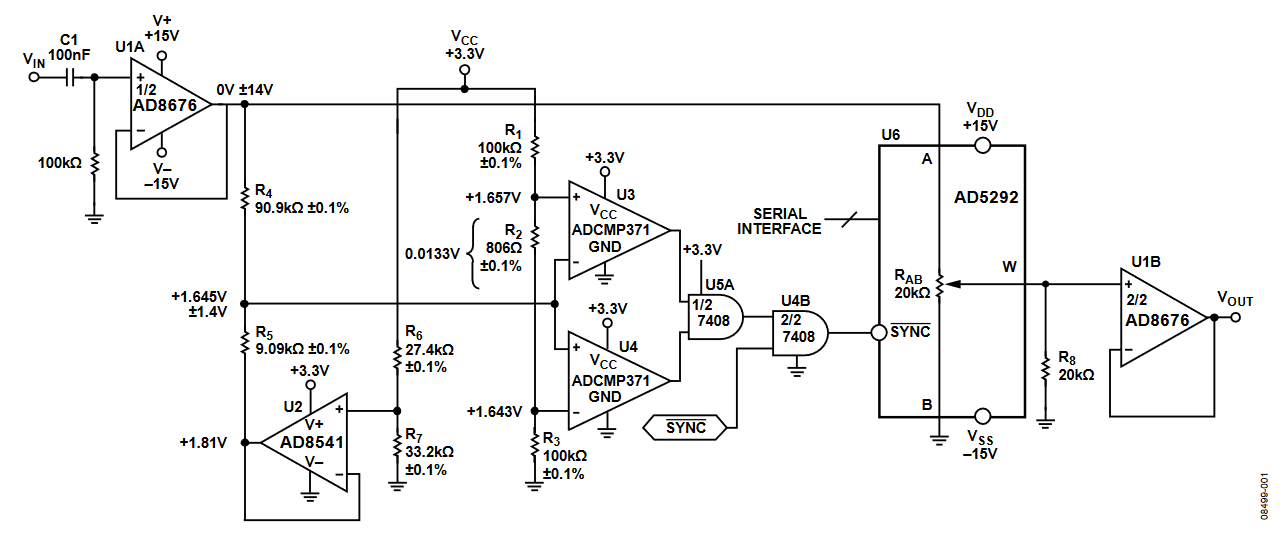
This circuit provides a logarithmic audio volume control with glitch reduction using the AD5292 digital potentiometer in conjunction with the dual AD8676 and single AD8541 op amps, ADCMP371 comparators, and 7408 AND gates.
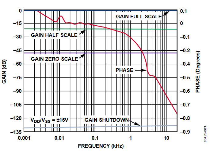
This circuit provides low total harmonic distortion (THD), a maximum signal attenuation of 46 dB, and a shutdown function that attenuates up to 130 dB, as shown in Figure 3. The AD5292 can be placed in shutdown mode by executing a software shutdown command. This feature places the RDAC in a special state in which terminal A is open-circuited and wiper W is connected to terminal B.
This circuit offers a logarithmic gain control function over an output voltage range of ±14 V (10 V rms) and is capable of delivering up to ±20 mA output current. The AD5292 is programmable over an SPI-compatible serial interface.
In addition, the AD5292 has an internal 20-times programmable memory that allows a customized volume setting at power-up.
This circuit provides low noise, low THD, high signal attenuation, low tempco, and high voltage capatibility. It is well suited for many audio applications.
Circuit Description

| Product | Description |
| AD5292 | Digital potentiometer, 10 bits, 1% resistor tolerance |
| AD8676 | Ultraprecision, dual, rail-to-rail output op amp |
| AD8541 | General-purpose CMOS, single, rail-to-rail amplifier |
| ADCMP371 | Comparator with push-pull output stage |
This circuit employs the AD5292 digital potentiometer in conjunction with the dual AD8676 and single AD8541 op amps, ADCMP371 comparators, and 7408 AND gates, providing a low distortion logarithmic audio volume control with glitch reduction. The logarithmic taper is achieved by adding resistor R8 between the wiper connection and ground. This method is described in detail in the article “Tack a Log Taper onto a Digital Potentiometer” by Hank Zumbahlen, EDN, 1/20/00.
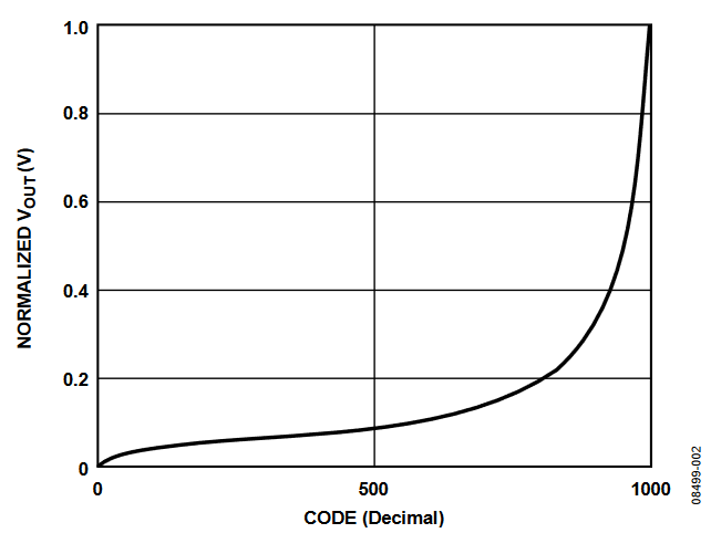
The circuit provides an input/output buffer, minimizing the load effects with other external circuits; the AD8676 dual op amp ensures low noise and precision rail-to-rail output voltage. Figure 2 shows the logarithmic output voltage, VOUT, normalized by VIN.

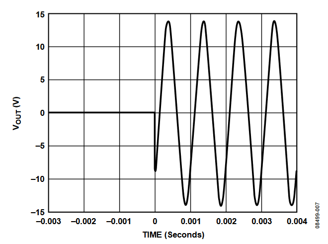
The audio volume control guarantees a maximum attenuation of 46 dB and up to 130 dB in shutdown mode. Figure 3 shows the attenuation for typical codes, including shutdown mode and signal phase delay, which is independent of the code.

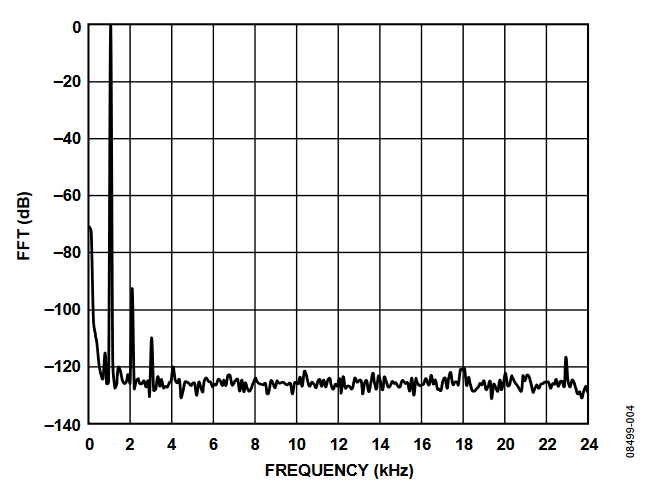
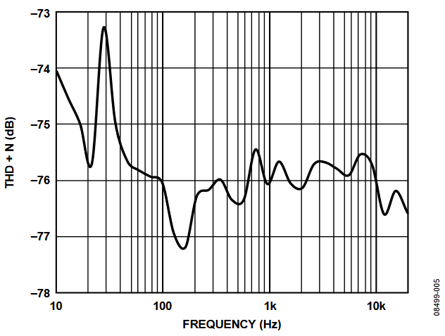
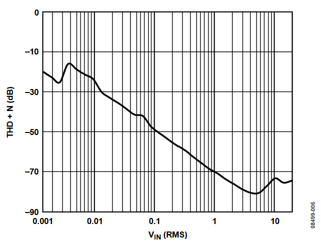
The circuit provides low total harmonic distortion, THD, typically −93 dB, as shown in Figure 4 for a 1 kHz, 1 VRMS input signal. Typical THD + Noise performance is shown in Figure 4, Figure 5, and Figure 6.


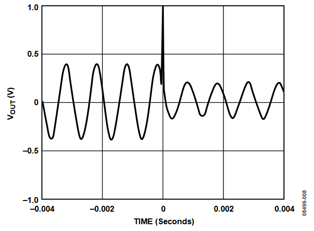
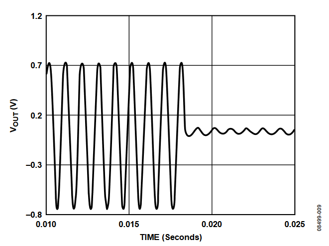
Without the glitch reduction circuit, the glitch due to a large attenuation step is shown in Figure 7, and the glitch due to the code transition of the internal switches is shown in Figure 8.


The glitch reduction circuit employs the AD8541, ADCMP371, and 7408 AND gates. Comparators U2 and U3 act as window comparators, with a 13.3 mV threshold between the two. This is large enough to overcome the typical comparator offset voltage.
This circuit is a zero crossing detector that minimizes the glitch by allowing the attenuation to change only when the signal is crossing 0 V. Resistors R4 and R5 attenuate the input signal by 90.91% and establish the common-mode voltage of 1.645 V into the window comparator. The maximum uncertainty of the zero crossing is approximately 133 mV reflected to the input. The output of the window comparator is AND'ed with the external SYNC command to drive the SYNC input of the AD5292. After the negative-going edge of SYNC to the AD5292, the next clock pulse updates the internal DAC register.
Resistors R1 to R7 should be 0.1% tolerance to ensure an optimal zero cross detection, which provides a smaller energy glitch and prevents large attenuation step. The threshold window is approximately 133 mV referenced to the input signal voltage, VIN. A typical attenuation step with glitch reduction circuit active is shown in Figure 9.

The AD5292 has 20-times programmable memory, which enables the user to preset the attenuation to a specific value at power-up.
Optimum layout, grounding, and decoupling techniques must be utilized in order to achieve the desired performance (see Tutorial MT-031 and Tutorial MT-101). As a minimum, a 4-layer PCB should be used with one ground plane layer, one power plane layer, and two signal layers.
Common Variations
The AD5291 (8 bits with 20-times programmable power-up memory) and AD5293 (10 bits, no power-up memory) are both ±1% tolerance digital potentiometers that are suitable for this application.
Learn More
Zumbahlen, Hank. "Tack a Log Taper onto a Digital Potentiometer," EDN, January 20, 2000.
MT-087 Tutorial, Voltage References. Analog Devices.
MT-091 Tutorial, Digital Potentiometers. Analog Devices.
MT-101 Tutorial, Decoupling Techniques. Analog Devices.
Data Sheets