Using Analog Devices SPI-compatible Display Drivers with other SPI Peripherals
要約
This application note discusses techniques to connect Analog Devices' daisy-chained SPI™-compatible display drivers and GPIO to 3-state SPI devices.
This application note discusses techniques to connect Analog Devices' SPI™-compatible display drivers to other SPI devices on a common SPI interface. The discussion applies to the MAX6950, MAX6951, MAX6952, MAX6954, MAX6957, and MAX7221 LED drivers, the MAX6850, and MAX6852 vacuum fluorescent display (VFD) controllers, and the MAX7301 general purpose I/O (GPIO) peripheral.
Motorola's serial peripheral interface (SPI) is a flexible synchronous serial interface superset standard. When implemented within a Motorola microcontroller such as one of the M68HC11 family, the SPI serial interface can be configured to send and receive data with a wide degree of flexibility of polarity and timing of the control signals. The operation of the microcontroller's serial interface is specified by configuration register. These register bits set clock polarity (CPOL) and clock phase (CPHA) as well as speed and detail timings for the serial transmissions. Table 1 shows the Analog Devices and Motorola nomenclature for the SPI interface functions.
| Analog Devices Pin Name | Analog Devices Pin Function | Connect to Motorola Pin Name | Motorola Pin Function | Implementation |
| DIN | Slave Data Input | MOSI | Master Output/Slave Input | ECH transmission is 16-bits |
| DOUT | Slave Data Output | MISO | Slave Output/Master Input | Expected to be a 3-state output |
| CS | Chip Select Input | SS | Slave Select Output | Set CPHA = 1 (chip/slave select line does not rise at end of each transmitted byte) |
| CLK | Master Clock Input | SCK | Clock Output | Set CPOL = 0 (slave samples data from master on rising edge of clock) |
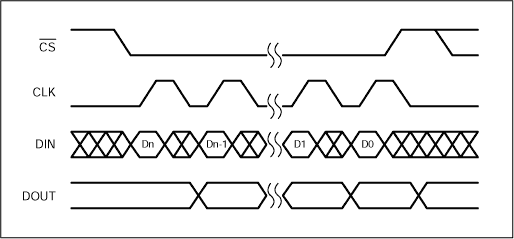
One issue that may arise is that the Motorola SPI protocol expects all slave devices to use 3-state MISO/DOUT outputs. This architecture allows multiple slaves to be connected to a common MISO/DOUT microcontroller input, and only an addressed slave drives the MISO/DOUT line at any time. The Analog Devices DOUT pin is, however, not 3-state. The reason for this was that multiple devices were expected to be daisy-chained (cascaded) together by connecting the DOUT of one device to the DIN of the next, and the CLK and CS lines of all devices being driven in parallel. This architecture reduces microcontroller pin count when large numbers of devices are being driven on one serial bus, because only one CS line is required. Since the DOUT of each device is likely to drive the DIN pin of another, the DOUT output remains active. If the DOUT output went high-impedance, the DIN input of a subsequent daisy-chained device would be high-impedance also. The difference between the behaviors is shown in Figures 1 and 2.

Figure 1. Motorola SPI interface timing (CPHA=1, CPOL=0).

Figure 2. Analog Devices SPI-compatible interface timing.
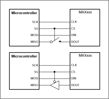
If the application demands that a mix of 3-state and non 3-state devices are mixed on the same SPI bus, the non 3-state devices can be converted to 3-state by adding an analog switch or a 3-state buffer between the DOUT pin and the SPI MISO pin (Figure 3). The analog switch or a 3-state buffer is gated on when CS goes low, selecting the device and enabling the DOUT at the same time.
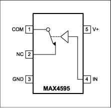
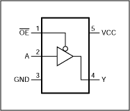
Suitable single analog switches are the pin compatible MAX4595 and MAX4502 in small SC-70 and SOT-23 packages (Figure 4). Alternatively, one third of a MAX4053 or 74HC4053 triple SPDT switch could be used. Suitable single 3-state buffers are the pin compatible Fairchild TinyLogic NC7SZ125 and TI SN74AHC1G125. The standard 74HC125 contains 4 such 3-state buffers in a single package.

Figure 3. Using an analog switch or 3-state buffer to create a 3-state DOUT.

Figure 4. MAX4595 and MAX4502 SPST analog switch pinout.

Figure 5. NC7SZ125 and SN74AHC1G125 pinout.
この記事に関して
製品
製造中
4線式インタフェース、2.5V~5.5V、20ポートおよび28ポートI/Oエキスパンダ
製造中
PWM輝度制御付き10ポート定電流LEDドライバおよびI/Oエキスパンダ
製造中
過電圧およびホットスワップ保護付き10ポートSPIインタフェースI/Oエキスパンダ
Serially Interfaced, +2.7V to +5.5V, 5- and 8-Digit LED Display Drivers
Serially Interfaced, +2.7V to +5.5V, 5- and 8-Digit LED Display Drivers
シリアルインタフェース、8桁、LEDディスプレイドライバ
4-Wire Interfaced, 2.7V to 5.5V, 4-Digit 5 x 7 Matrix LED Display Driver
4-Wire Interfaced, 7-, 14-, and 16-Segment Alphanumeric Vacuum-Fluorescent Display Controller
I/Oエキスパンダおよびキースキャン付き、4線式インタフェース、2.7V~5.5V、LEDディスプレイドライバ
4-Wire-Interfaced, 2.5V to 5.5V, 20-Port and 28-Port LED Display Driver and I/O Expander
4-Wire Interfaced, 5 x 7 Matrix Vacuum-Fluorescent Display Controller


