Triple Output LCD Power Supply Delivers 95% Efficiency from a Tiny 3mm x 3mm Package
Triple Output LCD Power Supply Delivers 95% Efficiency from a Tiny 3mm x 3mm Package
著者
John Bazinet
2004年05月01日
Introduction
Today’s handheld products pack more functionality in less space while demanding improved battery life over products of the previous generations. The only way to achieve both is to improve power efficiency in the device wherever possible. The color LCD display system is a good place to start, since it is an increasingly popular, but power hungry feature. The LTC3450 improves battery life and saves space by delivering a 95% efficient color LCD bias solution in a low profile (0.8mm tall), 3mm × 3mm package.
Figure 1 shows a block diagram of the LTC3450—a complete triple output LCD power converter—in a low noise 5.1V, 10mA output synchronous step up DC/DC converter. The charge pump based voltage tripler develops a 15V output and a voltage inverter develops −10V. The 15V and −10V outputs are used in the LCD display for VGL and VGH supplies, while the 5.1V output is used to provide the main panel power. The 5.1V converter switches at a constant 550kHz, which enables very low AVDD ripple voltage even when using tiny ceramic capacitors and one small inductor. The output voltages of the LTC3450 are sequenced to be compatible with color LCD displays with AVDD powering up first followed by VGL and then VGH.

Figure 1. LTC3450 block diagram.
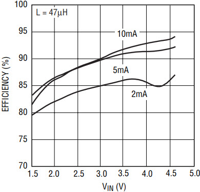
The LTC3450 also provides inrush current limiting during start-up (Figure 2), as well as output disconnect and active discharge in shutdown mode. The LTC3450 is stable with ceramic capacitors and its internal compensation eliminates the need for an external R-C compensation network. The LTC3450 also features a wide input voltage range of 1.5V to 4.6V, making it compatible with a wide variety of battery or fixed DC voltage inputs. Very low quiescent currents allow the LTC3450 to deliver excellent efficiency over the entire input voltage range (Figure 3).

Figure 2. AVDD turn on showing inrush current limiting.

Figure 3. LTC3450 AVDD efficiency vs VIN and load current.
Power Saving Mode
Some types of color LCD displays switch to an ultra low power state while the display is static, which allows for increased battery life. The LTC3450 supports this mode of operation by reducing its own quiescent current to a mere 30µA from the battery while maintaining all three regulated voltage outputs. This “Blank” mode operation is programmed via the Mode pin of the LTC3450. Driving the SHDN pin low reduces the LTC3450’s quiescent current to 10nA (typical) and all three voltage outputs are actively discharged to ground.
LCD Bias Power Supply Circuits
Figure 4 shows a 1.5V to 4.6V input to a triple output (5.1V/10mA, 15V/500µA and −10V/500µA) application circuit. Greater than 90% efficiency is maintained over the Li-Ion battery’s voltage range. This is far superior to an all charge pump approach that can only deliver efficiency approaching the LTC3450 when VIN is approximately 1/2 of AVDD.

Figure 4. 5.1V, 15V, −10V application circuit and efficiency.
Figure 5 shows a 1.5V to 4.6V input to 5.1V/10mA, 15V/500µA and −15V/500µA converter circuit. A tiny external dual diode is added to the circuit to get the converter to deliver the −15V and 15V outputs together.

Figure 5. 5.1V, 15V, −15V application circuit.
Figure 6 shows a 1.5V to 4.6V input to 5.1V/10mA, 15V and −5V circuit. Peak efficiency is greater than 90%. The magnitude of the negative output voltage (VGL) is equal to the positive voltage applied to VINV. VINV is connected to either AVDD (for −5V), V2X (−10V), or with the dual diode (Figure 4) for −15V. If desired, an independent positive voltage source between 5V and 15V can be connected to VINV to produce any desired negative voltage between −5 and −15V.

Figure 6. 5.1V, 15V, −5V application circuit.
Conclusion
The LTC3450 delivers a highly compact and efficient power supply solution for small LCD displays. Its wide input voltage range makes it easy to drop into a variety of applications. Built-in inrush current limiting, output disconnect and power saving controls simplify the task of implementing power friendly LCD displays.
著者について
John Bazinet has over 30 years experience as an architect, group director, strategist and developer of innovative, high performance power management solutions. He established and directed Linear Technology's New Hampshire ...


