The Evolution of High Voltage Digital Power System Management
The LTC3886 takes inputs up to 60V and produces two 0.5V-to-13.8V outputs—enabling it to easily drop into industrial, server and automotive environments as an intermediate or point-of-load (POL) supply. Other controllers with similarly impressive input/output ranges cannot match the LTC3886’s digital management capabilities. Its I2C-based PMBus-compliant serial interface allows power supply designers to configure, monitor, control and expand capabilities via PC-based, graphical LTpowerPlay® and then store optimal production settings in the LTC3886’s onboard EEPROM. No board changes are required, since capabilities and optimization settings (including compensation) can be changed via software.
This 2-channel PolyPhase® DC/DC synchronous step-down switching regulator controller employs a constant-frequency, current-mode architecture, with accurate input and output current sensing and programmable loop compensation, and is available in a 52-lead (7mm × 8mm) QFN package. Accurate voltage and current sensing, adjustable compensation and dedicated PGOOD pins make the LTC3886 ideal for industrial applications that demand versatile power system design, control, monitoring, programming and accuracy.
Flexible Feature Set
Figure 1 shows a generalized schematic of a LTC3886. The 100kHz to 750kHz PWM switching frequency range, and low RDS(ON) integrated N-channel MOSFET gate drivers support a plethora of external components and enable power capability and system cost optimization. The LTC3886 can readily accommodate a wide variety of industrial, medical, and point-of-load applications due to a flexible programmable feature set that addresses the specific application at hand.
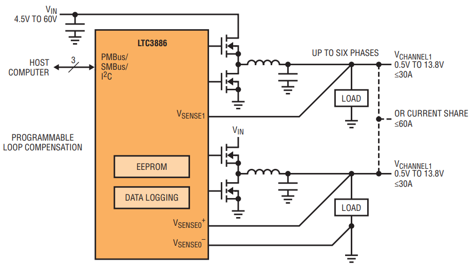
Figure 1. The LTC3886 is versatile and flexible. It features wide input and output ranges and and it is highly customizable via PMBus. Accurate telemetry is also available over the digital bus. All features can be controlled via LTpowerPlay.
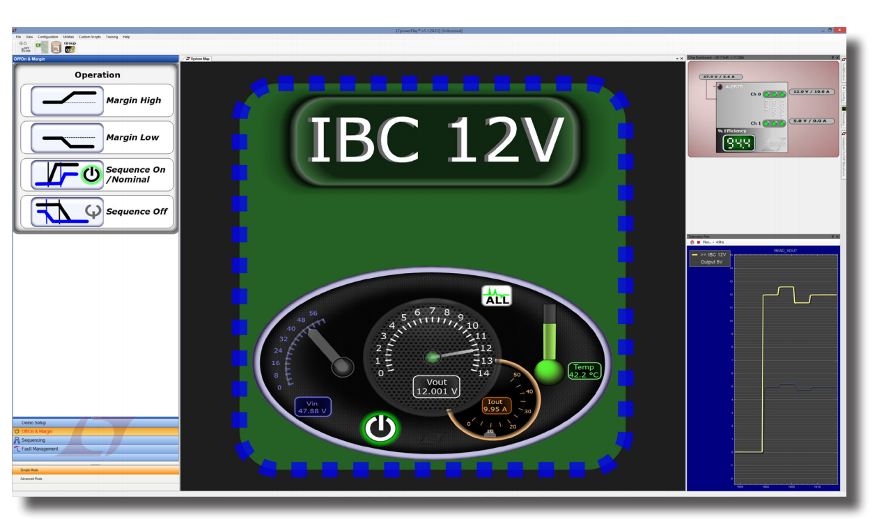
Figure 2. LTpowerPlay.
Adaptability Through Programmability
The following parameters of the LTC3886 are configurable and storable in the onboard EEPROM via the I2C/SMBus interface:
- Output voltage, overvoltage, undervoltage and overcurrent limit
- Input ON/OFF voltage, input overvoltage and input overcurrent warning
- Digital soft-start/stop, sequencing, margining
- Control loop compensation
- PWM switching frequency and phasing
- Fault response and fault propagation via the FAULT pins
- Device address
Switching frequency, device phasing and output voltage are also programmable with external configuration resistors. In addition, all 128 possible addresses are resistor selectable.
Power Good, Sequencing And Programmable Fault Response
The dedicated PGOOD pin for each channel simplifies enabling event-based sequencing across multiple LTC3886s and other power system management ICs. The LTC3886 also supports time-based sequencing. After waiting the TON_DELAY amount of time following the RUN pin going high, a PMBus command to turn on, or the VIN pin voltage rising above a preprogrammed voltage, the outputs are enabled.
| µModule Regulators | Controllers | ||||||||
| LTM4675 | LTM4676A | LTM4677 | LTC3880 | LTC3882 | LTC3883 | LTC3884 | LTC3886 | LTC3887 | |
| VOUT range (V) | 0.5–5.5 | 0.5–5.5 | 0.5–5.5 |
0.5–4.0, ch0 0.5–5.4, ch1 |
0.5–5.3 | 0.5–5.4 | 0.5–5.4 | 0.5–13.2 | 0.5–5.5 |
| VIN range (V) | 4.5–17 | 4.5–17 | 4.5–17 | 4.5–24 | 3.0–38 | 4.5–24 | 4.5–38 | 4.5–60 | 4.5–24 |
| VOUT accuracy (%) | 0.5 | 0.5 | 0.5 | 0.5 | 0.5 | 0.5 | 0.5 | 0.5 | 0.5 |
| Input current sense | calibrated | calibrated | calibrated | inferred | ✓ | ✓ | ✓ | inferred | |
| IOUT max (A) | dual 9 or single 18 | dual 13 or single 26 | dual 18 or single 36 | 30/phase1 | 40/phase1 | 30/phase1 | 30/phase1 | 30/phase1 | 30/phase1 |
| DCR sensing | NA | NA | NA | low | ultralow | low | very low | low | low |
| Digitally adjustable loop compensation | ✓ | ✓ | |||||||
| 1 Controller maximum IOUT depends on external components | |||||||||
Time-based power off sequencing is handled in a similar way. To assure proper time based sequencing, simply connect all SHARE_CLK pins together and connect together the RUN pins of all the power system management ICs. The LTC3886 FAULT pins are configurable to indicate a variety of faults including OV, UV, OC, OT, timing faults and peak current faults. In addition, the FAULT pins can be pulled low by external sources, indicating a fault in some other portion of the system. The fault responses of the LTC3886 are configurable and allow the following options:
- Ignore
- Shut Down Immediately—latchoff
- Shut Down Immediately—retry indefinitely at the time interval specified in MFR_RETRY_DELAY
Fault Logging And Telemetry
The LTC3886 supports fault logging, which stores telemetry and fault status data in a continuously updated RAM buffer. After a fault event occurs, the buffer is copied from RAM to EEPROM and becomes a persistent fault log, which can be read back at a later date to determine what caused the fault.
EXTVCC Pin For Maximum Efficiency
The EXTVCC pin is provided to minimize application power loss and supports voltages of 5V to 14V. It enables designs with optimal circuit efficiency and minimal die temperature, and enables the LTC3886 to efficiently supply its own bias power from the output voltage.
Accuracy And Precision
Modern applications require supply voltage regulation and supervision with stringent tolerances. These requirements are met with a high speed analog control loop and an integrated 16-bit ADC and 12-bit DACs. The output voltage accuracy of the LTC3886 is guaranteed at ±0.5% over the full operating temperature. In addition, the output voltage overvoltage and undervoltage comparators have less than ±2% error over temperature. The LTC3886’s regulation and supervision accuracy reduces total system costs with fewer output capacitors, while still meeting the tight input voltage requirements of downstream ICs.
The unique high side 60V input current sense amplifier measures the input current with less than ±1.2% error over temperature. The output current is guaranteed accurate to ±1.5% over temperature. The internal die temperature measurement of the LTC3886 is guaranteed accurate to 0.25°C, and the external temperature telemetry has less than ±1°C error.
Expansion
State of the art power management systems require increasing power and control, but must fit into dwindling board space. Parallel multiphase rails are the best solution for high power requirements because they enable high power density and efficient expandability. The LTC3886 supports accurate PolyPhase® current sharing for up to six phases between multiple LTC3886s. This allows system designers to add power stages as needed. In addition, the dual-phase LTC3870 PolyPhase expander IC mates seamlessly with the LTC3886 to create 6-phase PolyPhase rails at a lower price point. Figure 3 shows a 4-phase solution. Figure 4 shows the dynamic current sharing among the phases.
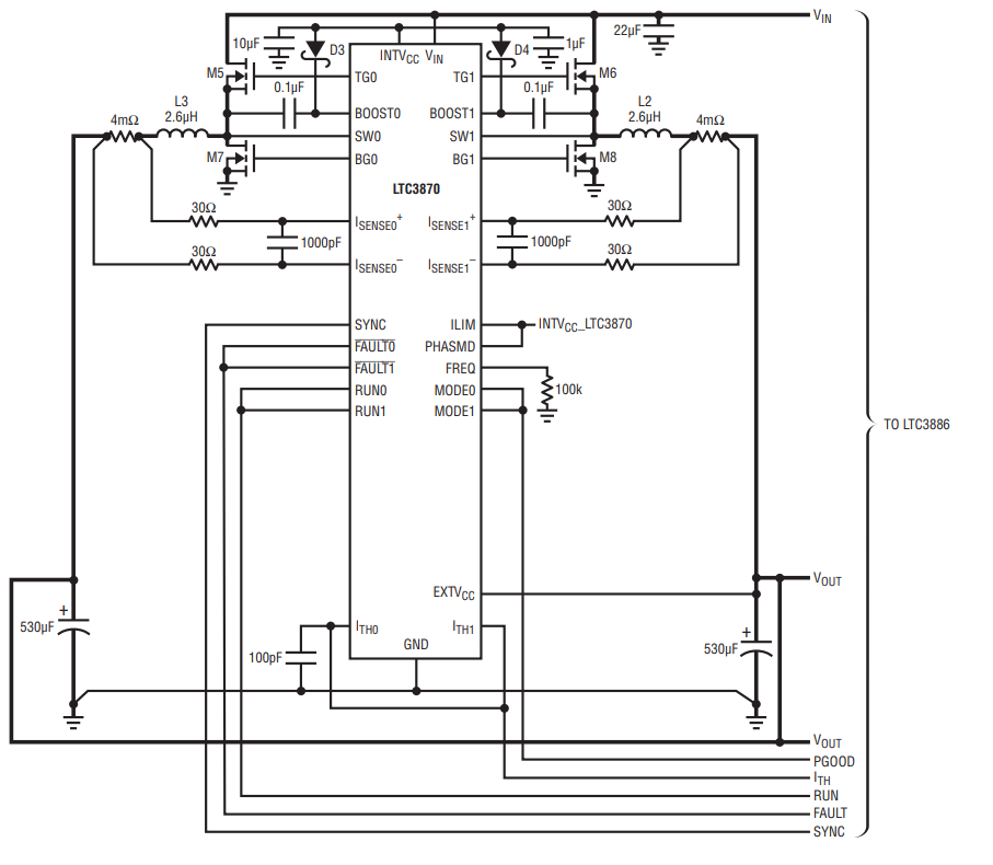
Figure 3. High efficiency 425kHz 4-phase, 48V input to 5V output, 50A step-down converter using the LTC3870 phase expander with the LTC3886.
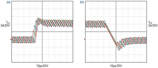
Figure 4. Dynamic current sharing for the 4-phase circuit shown in Figure 3; load step (a) rising and (b) falling.
The LTC3870 requires no additional I2C addresses, and it supports all programmable features as well as fault protection. When configuring a PolyPhase rail with multiple LTC3886/LTC3870s, the user simply shares the SYNC, ITH, SHARE_CLK, FAULTn, PGOODn and ALERT pins of all the channels connected to the rail. The relative phasing of all the channels should be set to be equally spaced. This phase interleaving results in the lowest peak input current and lowest output voltage ripple, and reduces input and output capacitor requirements.
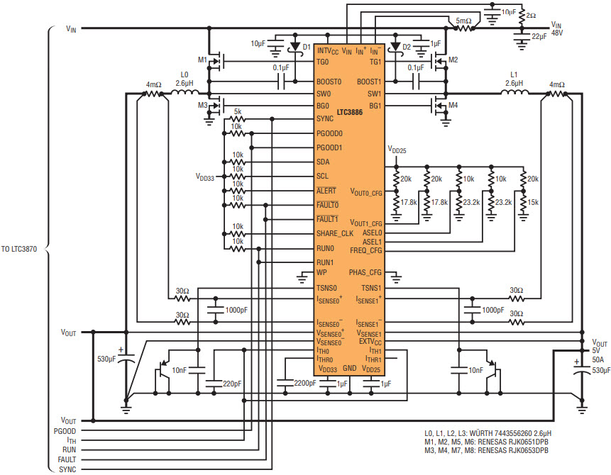
System architects often fragment the power system to meet functional and board space requirements: the LTC3886/LTC3870 PolyPhase rail simplifies fragmentation by breaking up the power and control components, allowing them to be easily placed in available spaces. Fragmentation also spreads the heat of the power supply system over the PCB, simplifying overall thermal extraction and reducing hot zones.
Progression
Figure 2 shows a screen from LTpowerPlay, a powerful Windows-based software development tool with graphical user interface (GUI) that fully supports the LTC3886. LTpowerPlay enhances evaluation when connected to demo boards and directly to application hardware. LTpowerPlay provides unparalleled development, diagnostic and debug features. Telemetry, system fault status and PMBus command values are all readily accessible through the GUI. The LTC3886 and other power system management ICs can be uniquely configured with ease using LTpowerPlay. Complete information is available at: : https://www.analog.com/en/design-center/ltpower-play.
Adjustable Compensation
The LTC3886 offers programmable loop compensation to assure loop stability and optimize the transient response of the controller without any external component changes. Gone are the days of painstakingly soldering and unsoldering multitudes of components to achieve the ideal compensation. A few clicks of a mouse using LTpowerPlay, and the LTC3886 can have optimal compensation. The control loop is fine-tunable quickly and painlessly, regardless of last minute component substitutions or variations. This empowers designers to squeeze the maximum performance out their systems by removing unnecessary output capacitors while saving board space and cost.
The process of programming loop compensation is summarized in Figures 5, 6 and 7. The error amplifier gm (Figure 5) is programmable from 1.0mmho to 5.73mmho using bits[7:5] of the MFR_PWM_COMP command, and the compensation resistor RTH, inside the LTC3886 is programmable from 0kΩ to 62kΩ using bits[4:0] of the MFR_PWM_COMP command. Only two external compensation capacitors, CTH and CTHP, are required in the design and the typical ratio between CTH and CTHP is set to a typical value of 10.
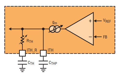
Figure 5. Programmable loop compensation.
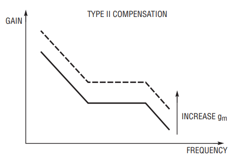
Figure 6. Error amp gm adjust.
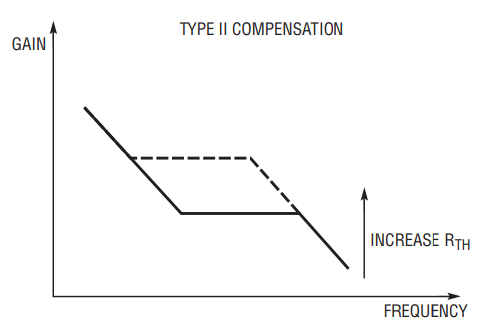
Figure 7. RTH adjust.
By adjusting the gm and RTH only, the LTC3886 provides a programmable type II compensation network for optimizing the loop over a wide range of output capacitors, and compensation component tolerances. Adjusting the gm of the error amplifier proportionately changes the gain of the compensation loop over the entire frequency range without moving the pole and zero location, as shown in Figure 6. Adjusting the RTH resistor changes the pole and zero location, as shown in Figure 7. Once the voltage and current ranges of the LTC3886 are determined, changes to the output voltage or current limit do not affect the loop gain. When the output voltage is modified by either changing voltage command, or by margining, the transient response of the circuit remains constant.
Accurate Telemetry For Optimizing System Efficiency With An Intermediate Bus
The LTC3886 has a wide input voltage range of 4.5V to 60V, and an output voltage range of 0.5V to 13.8V. This makes the LTC3886 an excellent choice for efficiently regulating a high voltage input supply voltage down to an intermediate bus voltage. The intermediate bus voltage powers downstream point-of-load converters (POL).
When used as an intermediate bus converter to power downstream power system management POLs, the LTC3886 enables the user to optimize the intermediate bus voltage for maximum efficiency. Since voltage and current telemetry provided by the LTC3886 and power system management ICs is so accurate, it is possible to produce accurate system efficiency measurements in real time. This, in turn, makes it possible to create an optimization program, in which a microcontroller determines the optimal intermediate bus voltage for various conditions.
To demonstrate this, a 9V-to-13V LTC3886 output intermediate supply was used to power the input of an LTM4676 8-phase demonstration circuit configured as a point-of-load converter, as shown in Figure 8. A Linear Technology Linduino® One demonstration board (www.analog.com/en/technical-articles/meet-linduino) measured and calculated the total efficiency of the system by reading the accurate voltage and current telemetry from the LTC3886 and LTM4676 via the PMBus. The Linduino application measured the total system efficiency at multiple intermediate bus voltages and modified the intermediate bus voltage for the lowest input power, achieving highest system efficiency, without user intervention.
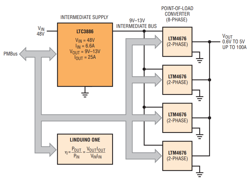
Figure 8. The LTC3886 set up as an intermediate bus to drive a power management IC POL converter. Telemetry from the LTC3886 intermediate supply and the POL ICs is used by a Linduino One demonstration circuit to optimize system efficiency by adjusting the intermediate bus voltage as load current changes.
The efficiency of the LTC3886 vs the intermediate bus voltage is shown in Figure 9. The total system efficiency vs the intermediate bus voltage is shown in Figure 10. The curves represent point-of-load currents of 10A, 20A, 40A, 80A and 100A, with the peak efficiency shifting respective of load current. Higher load currents require a higher intermediate bus voltage to operate at peak efficiency. Setting the intermediate bus voltage at a fixed voltage that is too high lowers the total efficiency of the system at low load currents. Compared to a using a standard fixed 12V intermediate bus voltage, optimizing the intermediate bus voltage with the LTC3886 improves efficiency by 6.2% at 10A of load current, 3.5% at 20A, and 1% at 40A. This technique enables efficiency optimization over the full workload of a system.
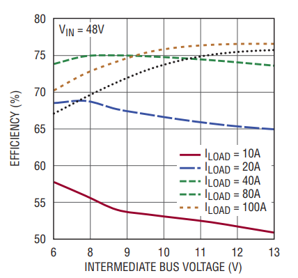
Figure 9. LTC3886 efficiency vs output.
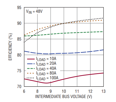
Figure 10. System efficiency.
Summary
The LTC3886 expands Linear’s portfolio of power system management controllers into the high voltage arena. A wide output voltage range of 0.5V to 13.8V, along with accurate voltage and current sensing, adjustable compensation, and dedicated PGOOD pins, gives LTC3886 users maximum design flexibility and performance. The LTC3886 is ideal for industrial applications that demand versatile power system design, control, monitoring, programming and accuracy.


