SOT-23 Switching Regulators Deliver Low Noise Outputs in a Small Footprint
SOT-23 Switching Regulators Deliver Low Noise Outputs in a Small Footprint
1999年02月01日
Introduction
As portable electronics designers continue to press for reduction in component sizes, Analog Devices introduces the LT1611 and LT1613 SOT-23 switching regulators. These current mode, constant frequency devices contain internal 36V switches capable of generating output power in the range of 400mW to 2W, in a 5-lead SOT-23 package. The LT1613 has a standard positive feedback pin and is designed to regulate positive voltages. The LT1611 has a novel feedback scheme designed to directly regulate negative output voltages without the use of level-shifting circuitry. Boost, single-ended primary inductance converters (SEPIC) and inverting configurations are possible with the LT1613 and LT1611. The high voltage switch allows hard-to-do, yet popular DC/DC converter functions like four cells to 5V, 5V to –5V, 5V to –15V or 5V to 15V to be easily realized.
Both devices switch at a frequency of 1.4MHz, allowing the use of tiny inductors and capacitors. Many of the components specified for use with the LT1613 and LT1611 are 2mm or less in height, providing a low profile solution. The input voltage range is 1V to 10V, with 2mA quiescent current. In shutdown mode, the quiescent current drops to 0.5µA. The constant frequency switching produces low amplitude output ripple that is easy to filter, unlike the low frequency ripple typical of pulse-skipping or PFM type converters. Internally compensated current mode control provides good transient response.
LT1613 Boost Converter Provides a 5V Output
Figure 1’s circuit details a boost converter that delivers 5V at 200mA from a 3.3V input. The input can range from 1.5V to 4.5V, making the circuit usable from a variety of input sources, such as a 2- or 3-cell battery, single Li-Ion cell or 3.3V supply. Efficiency, shown in Figure 2, reaches 88% from a 4.2V input. Start-up waveforms from a 3.3V input into a 47Ω load are pictured in Figure 3; the converter reaches regulation in approximately 250µs. The device requires some bulk capacitance due to the internal compensation network used. A 10µF ceramic output capacitor can be used with the addition of a phase-lead capacitor paralleled with R1; this capacitor is typically in the 10pF–100pF range.
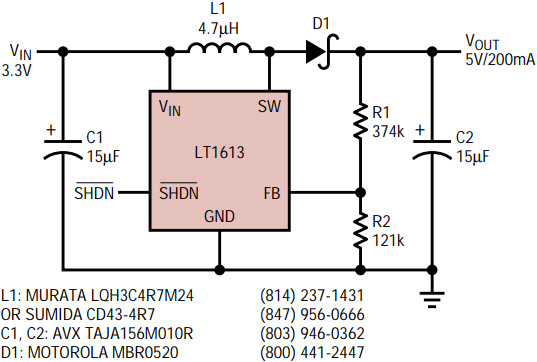
Figure 1. This boost converter steps up a 1.5V to 4.2V input to 5V. It can deliver 250mA from a 3.3V input.
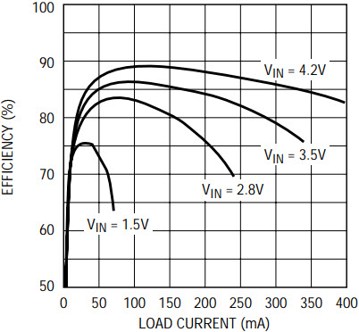
Figure 2. Efficiency of Figure 1’s boost converter.
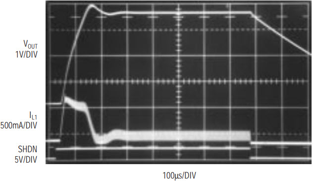
Figure 3. Boost converter start-up with 3.3V input into a 50Ω load.
LT1613 5V to 15V Boost Converter
By changing the value of the resistive divider, a 15V supply can be generated in a similar manner to the 5V converter shown in Figure 1. Figure 4 depicts the converter. L1’s value has been changed to 10µH to provide the same di/dt slope with a higher input voltage. The converter delivers 15V at 60mA from a 5V input, at efficiencies up to 85%, as shown in the efficiency graph of Figure 5.
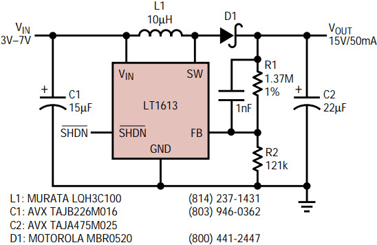
Figure 4. This 4-cell to 15V boost converter can deliver 50mA from a 3V input.
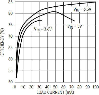
Figure 5. Efficiency of Figure 4’s circuit.
LT1613 4-Cell to 5V SEPIC
A 4-cell battery presents a unique challenge to the DC/DC converter designer. A fresh battery measures about 6.5V, above the 5V output, while at end of life the battery voltage will measure 3.5V, below the 5V output. Simple switching regulator topologies like boost or buck can only increase or decrease an input voltage, which will not do the trick in this situation. The solution is a SEPIC. A dual-winding inductor or two separate inductors are required to make this converter. Figure 6 details the circuit. A Sumida CLS62-150 15µH dual inductor is specified in the application, although two 15µH units can be used instead. Up to 125mA can be generated from a 3.6V input. Figure 7’s graph shows converter efficiency, which peaks at 77%. Transient response with a 5mA to 105mA load step is pictured in Figure 8. The converter settles to final value inside 200µs, with a maximum perturbation under 200mV. The double trace of VOUT under load in Figure 8 is actually switching ripple at 1.4MHz caused by the ESR of output capacitor C2. A better (lower ESR) output capacitor will decrease the output ripple.
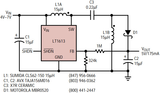
Figure 6. This single-ended primary inductance converter (SEPIC) generates 5V from an input voltage above or below 5V.
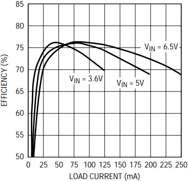
Figure 7. Efficiency of Figure 6’s SEPIC reaches 77%.
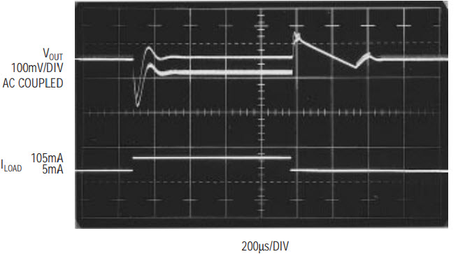
Figure 8. SEPIC transient response at 5V input with a 5mA to 105mA load step.
LT1611 5V to –5V Inverting Converter
A low noise –5V output can be generated using an inverting topology with the LT1611. This circuit, shown in Figure 9, bears some similarity to the SEPIC described above, but the output is in series with the second inductor. This results in a very low noise output. The circuit can deliver –5V at up to 150mA from a 5V input, or up to 100mA from a 3V input. Efficiency, described in Figure 10, peaks at 75%. Figure 11 illustrates the start-up waveforms. During startup, the switch-current increases to approximately 1A. At this current, the inductance of the Sumida unit decreases, resulting in the increased ripple current noticeable in the switch-current trace of Figure 11. After the circuit has reached regulation, the ripple current decreases by about a factor of two. Switching waveforms with a 100mA load are shown in Figure 12. Output voltage ripple is caused by ripple current in the inductor multiplied by output capacitor ESR.
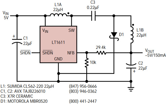
Figure 9. This inverting converter delivers –5V at 150mA from a 5V input.
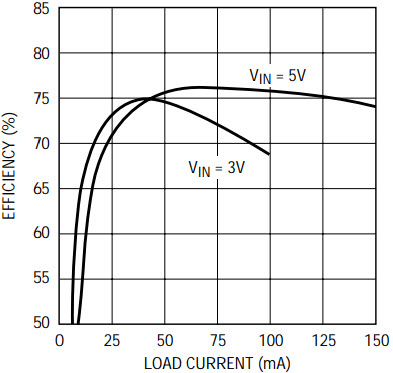
Figure 10. 5V to –5V inverting converter efficiency reaches 76%.
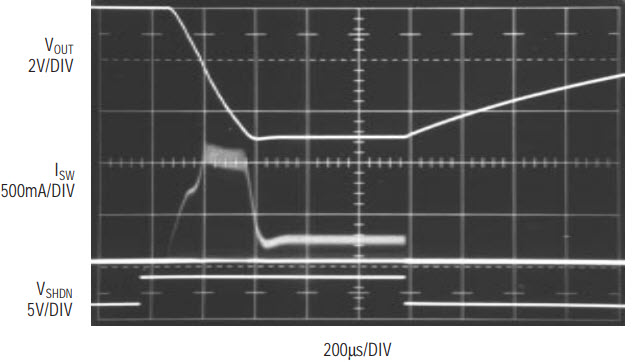
Figure 11. 5V to –5V inverting converter start-up into a 47Ω load.
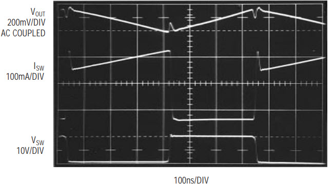
Figure 12. Switching waveforms of inverting converter with 100mA load.
Although the 20mVP-P ripple pictured in Figure 12 is low, significant improvement can be obtained by judicious component selection. Figure 13 details the same 5 to –5V converter function with better output capacitors. Now, output ripple measures just 4mVP-P. Additionally, transient response is improved by the addition of phase lead capacitor C5. Figure 14 depicts load transient response of a 25mA to 125mA load step. Maximum perturbation is under 30mV and the converter reaches final value in approximately 250µs.
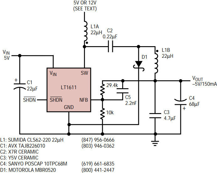
Figure 13. Low noise inverting converter; component selection and feedforward capacitor C5 reduce noise to 4mVP-P.
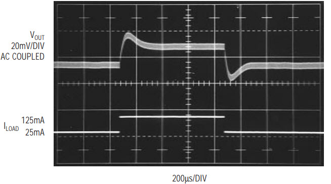
Figure 14. Transient response of low noise inverting converter is under 30mV for a 25mA to 125mA load step. Steady-state output ripple is 4mVP-P.
It is important to take notice of how Figures 9 and 13 are drawn. D1’s cathode is returned to the LT1611’s GND pin before both connect to the ground plane. This connection combines the current of the switch and diode, which conduct on alternate phases. The summation of both currents equals a current with no abrupt changes, minimizing di/dt induced voltages caused by the few nanohenries of inductance in the ground plane. This summed current is then deposited into the ground plane. If this technique is not followed, 100mV spikes can appear at the converter output (I speak from experience: my first several breadboards had this problem).
Many systems, such as personal computers, have a 12V supply available. Although the LT1611 VIN pin has a 10V maximum, the 36V switch allows a 12V supply to be used for the inductor while the LT1611’s VIN pin is still driven from 5V, as indicated in Figure 13. Significantly more output power can be obtained in this manner, as illustrated in the efficiency graph of Figure 15.
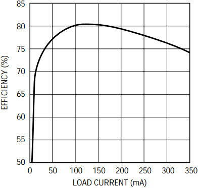
Figure 15. 12V supply at L1A increases efficiency to 81% and output current to 350mA.
LT1611 4-Cell to –10V Inverting Converter
A –10V low noise output can be generated in a similar manner as the –5V circuit described above. Figure 16’s circuit can deliver –10V at up to 60mA from a 3.6V input. Efficiency, graphed in Figure 17, reaches a high of 78%.
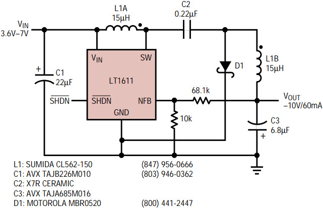
Figure 16. 4-Cell to –10V inverting converter delivers 75mA from a 4V input.
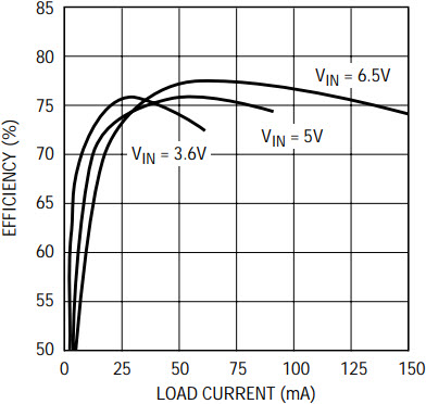
Figure 17. 4-cell to –10V converter efficiency.
Conclusion
The flexibility of individually controlled outputs in multiple-supply applications can make several LT1611/LT1613 converters attractive compared to a multiple-output flyback design with one large switching regulator and a custom transformer. Changing an output voltage on a multiple output flyback requires changing the transformer turns ratio, hardly a simple task. Conversely, individual control of each output, using the multiple LT1611/LT1613 approach, provides for complete control of each output voltage as well as supply sequencing. The LT1611 and LT1613 SOT-23 switchers provide small, low noise solutions to power generation needs in tight spaces.
著者について
Steve Pietkiewicz has served as Vice President, Power Management Products for Linear Technology since 2007. He was named General Manager, Power Products for Linear Technology in April 2005. From May 1995 to April 2005 he h...


