Smart Battery Charger Is Programmed via the SMBus
Introduction
Smart Batteries are becoming prevalent in the laptop computer world because they offer an industry-standard, high accuracy “gas gauge” system. These batteries conform to a set of specifications that define the operation of all of the components in a Smart Battery powered System (SBS). The battery has an embedded controller that tracks information related to battery charging and use. This information is provided to the system via a serial, 2-wire SMBus interface, a variant of the I2C™ bus in wide use today. The battery can be queried for information on remaining capacity, total capacity, time remaining at current rate of discharge, discharge current, terminal voltage and so on. Since most Smart Batteries can become a master on the bus, the battery can control the Smart Battery Charger for optimal charging. The LTC1759 Smart Battery Charger IC is designed to be controlled by this type of Smart Battery. In addition, a safety signal provided by the battery indicates whether the battery is present in the system and warns of possible thermal problems or battery faults if other systems fail. The emphasis of the SBS is on safety, ease of use and compatibility.
There are two types of Smart Battery Chargers (SBCs) allowed by the SBS specifications. A Level 2 charger, such as the LTC1759, is a slave on the SMBus and responds to commands from the battery to control charging. A Level 3 charger can be either a slave or a master on the SMBus, since it can query the battery to determine charging information. The SBC is independent of battery-chemistry type. It provides charging current and charging voltage in response to commands from the battery. Charge termination is sent by the battery as either zero current or zero voltage or as “terminate charge” alarm. Charging will also terminate if the safety signal indicates that the battery is not present or the battery is too hot to charge safely.
The LTC1759 is a complete Level 2 Smart Battery Charger. It is able to autonomously charge a Smart Battery by receiving and interpreting commands over its built-in SMBus interface. The LTC1759 adheres to all the safety requirements of the Smart Battery Charger Specification, including 3-minute timers that protect from SMBus communication failures and overcharging of Li-Ion batteries during wake-up mode—features absent from some competing solutions. Hardware-programmable current and voltage limits provide an additional level of protection that cannot be altered by errant software.
The LTC1759 manages all the complexities of a Smart Battery Charger System. This is appealing to those who wish to support Smart Batteries without getting involved in all the details. SBC compliance, safety, output voltage accuracy, SMBus accelerators and LTC’s patented wall adapter current limiting are just a few of the features that make this an outstanding part.
LTC1759 Smart Battery Charger Features
The LTC1759 merges the intelligence of a Smart Battery Charger with a constant-current (CC), constant-voltage (CV), current mode switching battery charger circuit. The LTC1759 incorporates the following features:
- 0.5% output voltage accuracy at room temperature, 1% over temperature range
- 5% output current regulation
- An external, resistor-programmable voltage limit, with four ranges that support stacking of the popular 4.2V battery cell
- An SMBus programmable output voltage, from 2.465V to 21V in either 16mV or 32mV granularity, depending upon the programmed voltage range (10-bit resolution)
- An external, resistor-programmable current limit with four limits: 1A, 2A, 4A and 8A
- An SMBus programmable output current with 10-bit resolution over all ranges
- LTC’s patented programmable AC wall adapter current limiting to maximize charge rate
- Low VIN-to-VOUT operation (dropout < 0.5V)
- 95% efficiency
- Compliant with Smart Battery Charger Specification Rev. 1.0, Level 2
- Low power consumption when AC is not present, while remaining compliant with all Smart Battery Charger requirements for status and interrupts
- Built-in SMBus accelerators (similar to the LTC1694)
- New 36-pin narrow SSOP package (0.209˝ wide)
Circuit Description
The LTC1759 is composed of a synchronous, current mode, PWM step-down (buck) switcher controller, a charger controller, two 10-bit DACs to control charger parameters, a thermistor Safety Signal decoder, hardware voltage and current limit decoders and an SMBus controller block (refer to Figure 1).
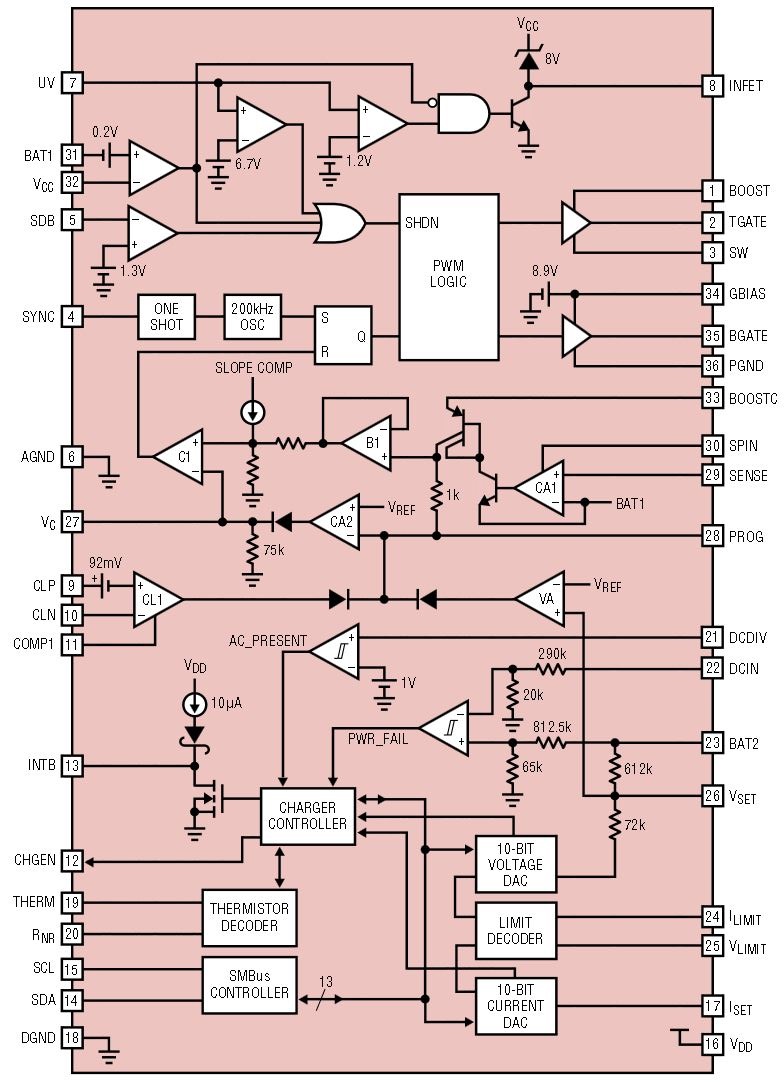
Figure 1. LTC1759 block diagram.
The Smart Battery or system controller programs both constant-current (CC) and constant-voltage (CV) limit values though commands over the SMBus interface. The buck converter uses N-channel MOSFETs for switches, allowing low cost, high efficiency operation. It also provides reverse battery discharge protection and ultralow dropout operation. A thermistor safety-detection circuit is used to detect the presence of a battery and determine whether the temperature of the battery allows safe charging to occur. Analog Devices' patented input current limiting feature is implemented, allowing the fastest battery charge times without overloading the wall adapter.
When a constant current value is received via an SMBus transmission, it is scaled and limited to a value below that programmed by the RILIMIT resistor. This modified value programs the current DAC, setting the DC charging current. The current DAC is a 10-bit delta-sigma DAC that sinks current from the PROG pin when charging current is desired (refer to Figure 2). Amplifier CA1 senses the voltage drop across RSENSE and forces this voltage across RS2 (200Ω); the current through RS2 is sent through a current mirror as a pull-up current on the PROG pin. The matching of current through RS2 with current from the PROG pin by CA2 implements constant-current operation. Since the delta-sigma DAC output is a series of pulses, a smoothing capacitor is needed to filter the pulses into DC.
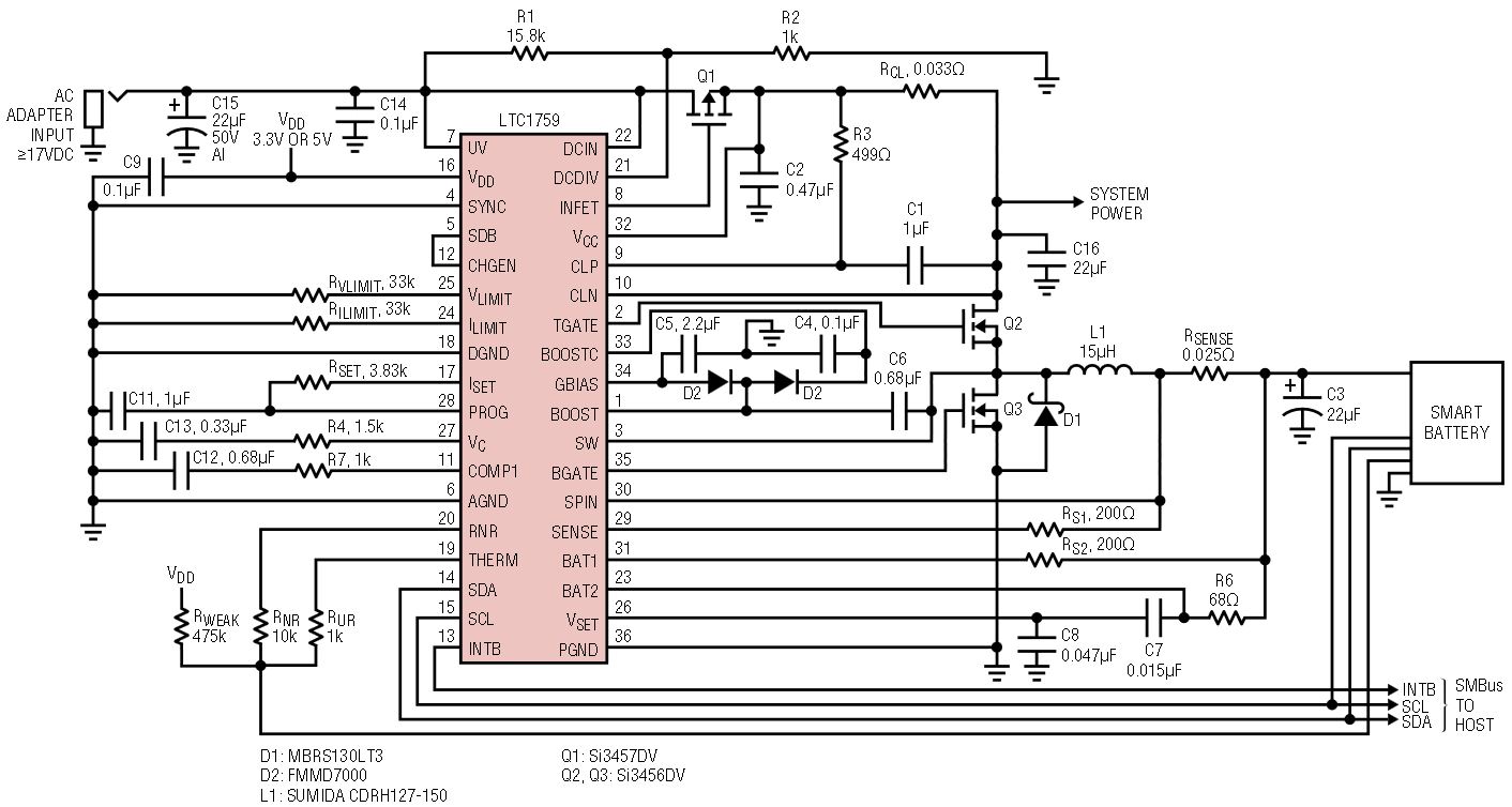
Figure 2. A complete 4A Smart Battery Charger.
When a constant-voltage value is received via an SMBus transmission, the value is scaled, adjusted to cancel offset and limited to a value below that programmed by the RVLIMIT resistor. This modified value programs the voltage DAC, setting the DC charging voltage. The voltage DAC drives the bottom of an internal voltage divider network. The top of the voltage divider is connected directly to the battery output though the BAT2 pin. A voltage error amplifier, VA, compares the divided battery voltage on the VSET pin with an internal, precision reference voltage. The output of the VA amp is configured as a current source that can drive the PROG pin. The PROG pin is a current summing node for both current and voltage feedback loops. The VA loop steals control of the current feedback loop when the battery voltage exceeds the programmed voltage, forcing the charging current down to the level required to maintain the programmed voltage. Since the ΔΣ DAC output is in the form of a series of pulses, a smoothing network is needed to filter the pulses into DC at the VSET pin. The capacitors C5 and C4 form a capacitance divider that provides some filtering of the feedback voltage from the battery while filtering the DAC pulses.
The LTC1759 requires two power supplies. The PWM circuitry runs directly off the wall adapter supply through the VCC pin, whereas the logic functions run independently from the VDD supply. This allows the PWM circuitry to go into 40µA micropower shutdown mode when AC power is removed, allowing the logic and SMBus activity to remain alive, as required by Intel’s ACPI standards. This separate supply also allows the logic and SMBus to run at 3V or 5V depending on the system designer’s needs. To minimize power draw of the LTC1759 logic, the logic circuits are driven by a clock circuit that shuts down when there is no activity and wakes up to service SMBus activity or to generate interrupts. Once the request is serviced, the LTC1759 goes back to sleep.
Shutdown of the PWM through the CHGEN–SDB pin combination occurs when the AC power is lost or the battery is removed. The LTC1759 detects the AC loss through the DCDIV pin. This threshold is usually set just below the lowest valid voltage of the wall adapter. AC power status may be read by the system over the SMBus. The UV pin is only used to put the PWM circuitry into micropower shutdown and is connected directly to the wall adapter supply.
Inductor selection is not critical with the design, since the loop response of the charger is intentionally set to be very slow. Almost any value will work, with a practical lower limit of about 15µH. Lower inductance will create higher ripple currents, requiring a lower ESR capacitor on the output. It will also cause cosmetically ugly discontinuous switching operation to occur at higher currents than necessary.
Output capacitor selection is not ESR critical but must be able to handle all of the ripple current from the charger. Do not count on the battery to carry the ripple current because the effective impedance as seen by the charger can be much greater than the ESR of the capacitor. Many battery packs have built-in series-protection MOSFETs that raise the ESR of the battery. There may also be optional power-routing MOSFETs in series with the battery in multiple-battery configurations, further increasing the battery ESR. From the charger point of view, the output capacitor ESR can be as high as 1Ω, allowing a wide range of capacitor options. When using a resistive or electronic load, some instability may occur. This can be fixed by adding a temporary 300Ω resistor in series with the PROG pin capacitor or putting a 10µF capacitor on the output. Avoid using ceramic capacitors in the output because they tend to make noise when the switcher goes discontinuous and starts to drop cycles at audible frequencies under very light load currents—use tantalums instead. Input capacitance selection is driven by the input ripple current of the charger, which is usually 1/2 of the maximum output current. For a 4A charger, a 22µF, 50V ceramic is recommended, since this part can typically handle 2A of ripple current. It also takes up the least amount of space and can cost less than other capacitor options.
Current protection, from battery to wall adapter, is provided by a P-channel MOSFET (Q1). A voltage comparator monitors the voltage across the MOSFET and will turn it off when the wall adapter drops to less than 200mV above the battery voltage. Although an inexpensive diode could be used instead of this MOSFET, the MOSFET only adds 100mV to the already low 0.4V dropout mode of operation without producing extra heat. During startup without a battery, the MOSFET parasitic diode is used to allow wall adapter power to reach the VCC pin and power up the PWM control circuitry.
Primary compensation is done on the PROG pin; however, DAC pulse filter requirements determine the effective value of the capacitor. Pulse ripple current must be less than 20mV or loop jitter will occur, giving the appearance of loop instability at light charging currents. The VC pin capacitor’s primary function is to provide soft-start support. There must always be a resistor of 1.5k in series with the VC pin capacitor to allow proper shutdown.
From a thermal standpoint, the output voltage remains approximately 0.5% accurate over the battery temperature charging range. This higher precision allows a higher charge capacity in the battery, and, more importantly, will cause fewer problems with voltage-based charge termination circuitry in the battery.
SMB Alert
The SBS standards allow for the option of an open-collector interrupt line to notify the host when a critical power event has occurred. This feature is called SMBALERT#. The LTC1759 implements this feature by asserting the INTB line low when AC power is lost or restored and when a battery is physically installed or removed. INTB is cleared when the host reads the LTC1759 status register or performs a successful read of the SMBALERT# Response address of the LTC1759.
Setting Safe Voltage and Current Ranges
The LTC1759 voltage/current ranges are programmed with two external resistors, RVLIMIT and RILIMIT, as shown in Tables 1 and 2. These limits prevent communication errors or errant software from causing the charger to damage the battery. At the same time, the variable granularity allows for better control of voltage and current in the lower ranges. The voltage limits are ROM mask programmable.
| RILIMIT | Nominal Charging Current Range | Granularity |
| 0Ω | 0 < I < 1023mA | 1mA |
| 10k | 0 < I < 2046mA | 2mA |
| 33k | 0 < I < 4092mA | 4mA |
| Open (>250k) or shorted to VDD | 0 < I < 8184mA | 8mA |
| RVLIMIT | Nominal Charging Voltage (VOUT) Range | Granularity |
| 0 | 2465 < VOUT < 8432mV | 16mV |
| 10k | 2465 < VOUT < 12,640mV | 16mV |
| 33k | 2465 < VOUT < 16,864mV | 32mV |
| 100k | 2465 < VOUT < 21,056mV | 32mV |
| Open or tied to VDD | 2465 < VOUT < 32,768mV | 32mV |
SMBus Acceleration
Unlike the I2C bus, which allows the use of variable pull-up currents on the bus signals, the SMBus pull-up current is specified as a maximum of 350µA. In larger systems, the capacitance load on the SMBus can cause rise-time violations (TRISE > 1µs), which could result in a communication failure. This is especially the case when I2C devices are mixed with SMBus-compliant devices on the same bus. The thresholds of the I2C bus receivers are generally higher than their SMBus cousins and are more sensitive to slow rise times.
Both SCL and SDA have dynamic pull-up circuits that improve the rise time on systems with significant capacitance on the two SMBus signals. The dynamic pull-up circuitry detects a rising edge on SDA or SCL and applies 2mA–5mA pull-up to VDD for approximately 1µs (Figure 3). This action allows the bus to meet SMBus rise-time requirements with as much as 150pF on each SMBus signal. The improved rise time will benefit all of the devices that use the SMBus line, especially devices that use the I2C logic levels.
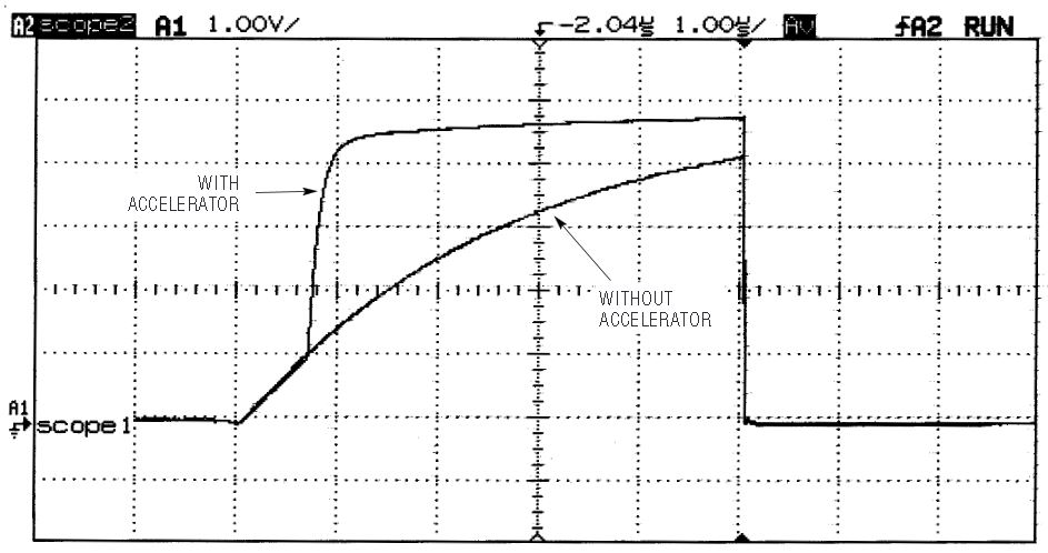
Figure 3. SMBus accelerator operation (RPULLUP = 15k, CL =150pF, VDD = 5V).
AC Adapter Current Limiting
Wall adapters are typically AC/DC converters with 20V output at 3A–4A of load current. When a notebook is running, all of the available current from the wall adapter may be consumed by the system, leaving no power for charging the battery. However, as soon as the system’s power requirements drop below the wall adapter’s current limit, battery charging can resume. In order to recharge the battery in the shortest time possible, the recharging should start as soon as there is any current leftover from the system. The ideal situation is when the sum of battery charging current and the system current is just below the wall adapter’s current limit. The LTC1759 incorporates a patented battery charger input current-limiting function that allows the charger current to be automatically reduced to avoid overloading the wall adapter, yet still charge the battery with the maximum available current.
Improved Safety Signal Sensing
The Safety Signal in most Smart Batteries is a resistor or thermistor to the battery’s negative terminal. The SBC must sense the resistance of the Safety Signal to ground and determine if the battery is connected and whether it is safe to charge. The SBC must report the status of the Safety Signal during an SMBus read of the ChargerStatus() register. Table 3 shows the five ranges of resistance and what the ChargerStatus() bits must indicate.
| Safety Signal Resistance | ChargerStatus Bits | Description |
| 0Ω–500Ω | SAFETY_UR = 1 SAFETY_HOT = 1 BATTERY_PRESENT = 1 |
Underrange |
| 500Ω–3k | SAFETY_HOT = 1 BATTERY_PRESENT = 1 |
Hot |
| 3k–30k | All Safety Bits Clear BATTERY_PRESENT = 1 |
Ideal |
| 30k–100k | SAFETY_COLD = 1 BATTERY_PRESENT = 1 |
Cold |
| >100k | SAFETY_OR = 1 SAFETY_COLD = 1 BATTERY_PRESENT = 0 |
Overrange |
The LTC1759 monitors the safety signal using a state machine to control the thermistor sensing scheme of Figure 4. This approach allows the LTC1759 to conserve power while supporting battery-presence detection and safety signal reporting when AC is not present. It also provides high noise immunity at the underrange-to-hot trip point.
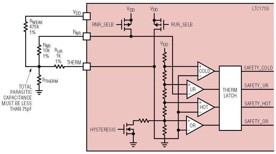
Figure 4. LTC1759 safety-signal-monitoring circuitry.
The state machine sequentially switches RWEAK, RNR and RUR to pullup against the battery’s internal thermistor. The resulting voltage is monitored by the comparators and used to determine the thermistor’s operating range. The state machine is able to sample the safety signal with all three resistors in 100µs. This allows the thermistor to be read during an SMBus read requesting Safety Signal status and then shut down to conserve power. A system using a fixed 10k pullup for all ranges will waste current when AC is not present. RWEAK is used to continuously monitor battery presence; it uses very little current and allows detection of the insertion or removal of a battery regardless of whether or not AC is present. RNR is used to determine if the safety range is cold or ideal. RUR is used to determine if the safety range is hot or underrange. The testing of RTHERM is shown for a cold and underrange thermistor in Figures 5 and 6, respectively. When AC is present, the state machine continuously tests the thermistor every 100µs. When AC is not present, RNR and RUR thermistor testing occurs only when a battery is first inserted or removed or during a transmission requesting Safety Signal status.
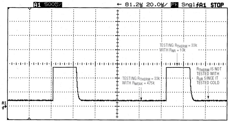
Figure 5. Testing a cold thermistor.
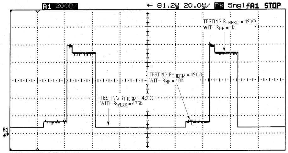
Figure 6. Testing an underrange thermistor.
The underrange detection scheme is a very important feature of the LTC1759. As can be seen from Figure 6, the RUR/RTHERM trip point of 0.333 • VDD (1V) is well above the 0.047 • VDD (140mV) threshold of a system using a 10k pull-up for all ranges. A system using a 10k pull-up would not be able to resolve the important underrange-to-hot transition point with a modest 100mV of ground offset between the battery and thermistor-detection circuitry. Such offsets are anticipated when charging at normal current levels.
Conclusion
The LTC1759 complies with the Smart Battery Charger standard published by the Smart Battery System organization, in which Analog Devices is a promoter and voting member. The charger controller also complies with Intel’s ACPI standard by being able to respond to system commands even when there is not AC wall adapter power. The charger offers the widest current and voltage range of operation compared to competitive parts. Feature for feature, it also offers the highest integration possible today with a Smart Battery Charger. The LTC1759 achieves significant cost savings, performance and safety advantages over other Smart Battery Chargers currently available.
Notes
I2C is a trademark of Philips Electronics N.V.


