概要
このアプリケーションノートでは、Power over Ethernet (PoE)アプリケーションのための、IEEE 802.3af準拠の受信機器(PD)モジュールを紹介します。MAX5941B PoEインタフェース/PWMコントローラを用いたこのモジュールは、検出シグネチャ、構成可能な分類シグネチャ(オプション)、プログラム可能な低電圧ロックアウト(UVLO)を備えたPD、およびプログラム可能な突入電流制御付きアイソレーションスイッチを提供します。
MAX5941B PDモジュールは12cm²のPCB上に実装され、ホットスワップ電力スイッチング、DC-DCコンバータ、および一対のORingダイオードブリッジを内蔵し、12Vの外部アダプタに対応しています。つまり、IP電話、ワイヤレスアクセスノード、およびセキュリティカメラなどのPDに、固定周波数のDC-DC絶縁電源を実装するのに必要なすべての機能を提供します。
標準的なアプリケーション
MAX5941B PDモジュールは、数多くのアプリケーションで使用することができます。図1では、スイッチから出力されたデータがミッドスパンの入力に接続される代表的なアプリケーションを示しています。その後、ミッドスパンはPoEをサポートする各出力上のデータに電力を供給します。
この例では、ポート1にEthernetカメラを接続し、ポート2にワイヤレスアクセスポイントを接続しています。ミッドスパンのスイッチをオンにすると(あるいは機器を接続すると)、ミッドスパンは各出力をチェックしてPoEシグネチャの有無を確認します。モジュールは、ポート1とポート2の周辺機器をPoE対応機器として識別し、ミッドスパンはこれらの周辺機器にデータと電力の両方を供給します。
ミッドスパンは、PoE対応の機器が追加されたか外されたかを確認するため、絶えず各出力を監視しています。この例では、他のポートにPoEシグネチャがないため、ミッドスパンは接続された周辺機器にデータのみ渡します。
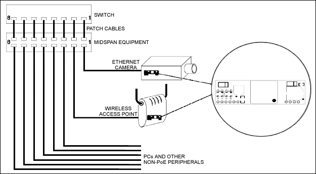
図1. 標準的なアプリケーションでは、スイッチから出力されるデータはミッドスパンに接続されます。これによって、電力がデータに追加され、Ethernetを介して電力が供給されます。
特長
- IEEE 802.3af準拠
- 36V~60Vの入力電圧範囲
- 12V/1A出力
- 最小負荷要件がない
- 小型SILパッケージサイズ
- 出力リップルおよびノイズが小さい
- 高効率の受電機器
- 外付けコンデンサが不要
- 出力電圧が調整可能
- 低コスト
- 1500V絶縁(入力から出力まで)
- 12Vの外部ACアダプタで使用するオンボードORingダイオード
端子説明
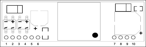
図2. ピン配置
| Pin Number | Name | Description |
| 1 | VA1 | Rx Input (1) This input pin is used in conjunction with VA2 and connects to the center tap of the transformer connected to pins 1 and 2 of the RJ45 connector (Rx)—it is not polarity sensitive. |
| 2 | VA2 | Tx Input (2) This input pin is used in conjunction with VA1 and connects to the center tap of the transformer connected to pins 3 and 6 of the RJ45 connector (Tx)—it is not polarity sensitive. |
| 3 | VB1 | Direct Input (1) This input pin is used in conjunction with VB2 and connects to pins 4 and 5 of the RJ45 connector—it is not polarity sensitive. |
| 4 | VB2 | Direct Input (2) This input pin is used in conjunction with VB1 and connects to pins 7 and 8 of the RJ45 connector—it is not polarity sensitive. |
| 5 | CP1 | Class Programming (1) Connecting an external resistor to CP2 will change the current class of the module. With no resistor fitted the module will default to Class 0. |
| 6 | CP2 | Class Programming (2) Connecting an external resistor to CP1 will change the current class of the module. With no resistor fitted the module will default to Class 0. |
| 7 | GND | Ground The ground return for the output. |
| 8 | VOUT | DC Output This pin provides the regulated output voltage from the DC-DC converter. |
| 9 | ADJ | Output Adjust The output voltage can be adjusted from its nominal output by connecting an external resistor from this pin to either the VOUT pin or GND pin. |
| 10 | N.C. | No Connection This pin is not connected internally. |
電力分類
電力分類は、PDが給電機器(PSE)に電力要件を示すためのオプションの方法です。図3に示すように、MAX5941Bモジュールは、CP1とCP2のピンの間に抵抗を接続することによって、外部から電流クラスをプログラムすることができるようにしています。抵抗を装着しない場合、モジュールはデフォルトでクラス0に設定されます。表2はプログラム抵抗値の全リストです。
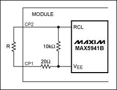
図3. 電力区分を設定するためにピンCP1とCP2の間に抵抗を接続
| Class | Programming Resistance (Ω) | Minimum Power (W) | Maximum Power (W) |
| 0 | Do not fit | 0.44 | 12.95 |
| 1 | 770 | .44 | 3.84 |
| 2 | 388 | 3.84 | 6.49 |
| 2 | 388 | 3.84 | 6.49 |
| 3 | 242 | 6.49 | 12.95 |
| 4 | 161 | Reserved | Reserved |
出力調整
MAX5941b pdモジュールは、公称値から上下にずれる出力電圧を調整する、adjピンを備えています。出力電圧を調整するには、adjピンと、gndピンまたはVOUTピンのいずれかの間に抵抗を接続します(図4)。式1および式2は、所望の出力電圧を上下に調整するのに必要な抵抗値を算出しています。

ここで、VTRIM_UPは、上側に調整される所望の出力電圧で、VTRIM_DOWNは、下側に調整される所望の出力電圧です。
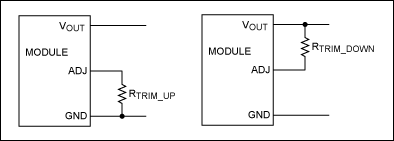
図4. 出力電圧を調整するには、ADJとGND (上側に調整)、またはADJとVOUT (下側に調整)の間に抵抗を接続します。
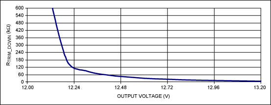
図5A. 上側に調整された出力電圧曲線
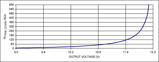
図5. 下側に調整された出力電圧曲線
12Vの外部アダプタを備えた標準的な接続
従来、図6に示すように、PDはアダプタを同時に使用し、ダイオードは各出力端に直列に接続します。
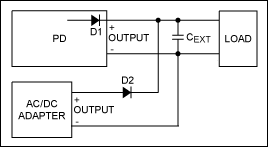
図6. 従来のソリューションでは、ダイオードを各出力端に直列に配置した状態で、受電機器をアダプタに接続します。
MAX5941B PDモジュールでは、出力ダイオードD1は内蔵されています。PDを独立して使用する場合、効率を向上するために、ダイオードを0Ω抵抗に交換します。図7はボード上のORingダイオードD1の配置を示します。
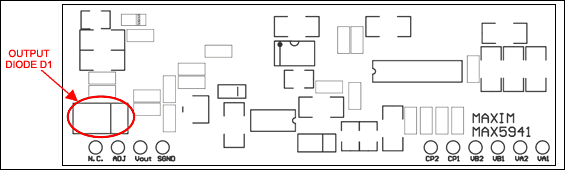
図7. MAX5941B PDモジュール上の内部ダイオードD1の位置
The module only requires one external capacitor, as shown in Figure 8; minimally, a 1µF ceramic capacitor is recommended.
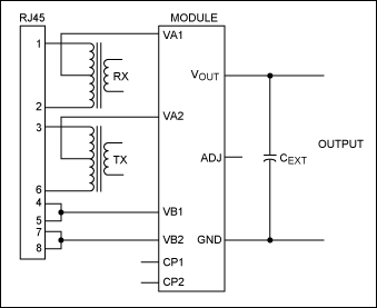
図8. GNDとVOUTの間に外付けコンデンサを接続した状態の標準的な接続図
電気的特性
| Parameter | Min | Typ | Max | Units |
| DC Supply Voltage | -.3 | 60 | V | |
| DC Supply Voltage Surge for 1ms | -.6 | 80 | V | |
| Storage Temperature | -40 | +100 | °C |
「絶対最大定格」に挙げた値を超えるストレスが加わると、モジュールに永久的な損傷を生ずるおそれがあります。これらの値はストレス定格専用であり、ここに示された条件またはそれを超えるその他のいかなる条件においてもモジュールが正しく機能することを示すものではありません。長期間、絶対最大定格条件下に晒されると、モジュールの信頼性に影響する可能性があります。
| Parameter | Min | Typ | Max | Units |
| Input Supply Voltage | 36 | 48 | 60 | V |
| Undervoltage Lockout | 30 | 36 | V | |
| Operating Temperature | -40 | 25 | +85 | C° |
| Parameter | Min | Typ | Max | Units |
| Nominal Output Voltage (Without the ORing Diode) | 11.76 | 12 | 12.24 | V |
| Output Current | 0 | 1 | A | |
| Output Ripple and Noise | 250 | mV | ||
| Efficiency Without the ORing Diode (48V Input, 1A Output) | 85 | % | ||
| Efficiency with the ORing Diode (48V Input, 1A Output) | 82 | % | ||
| Isolation Voltage | 1500 | V |
波形
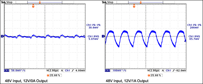
図9. 出力リップルとノイズ
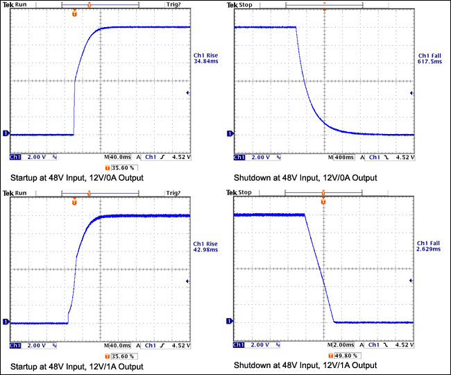
図10 起動とシャットダウン
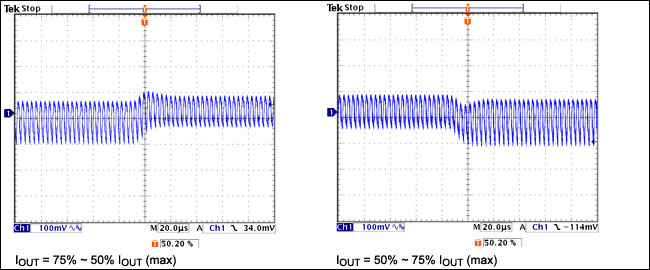
図11. 負荷過度応答
部品リスト
| Designation | Qty | Description |
| C1, C2, C6, C17 | 4 | 10µF 25V ceramic capacitor 1206 TDK C3216X5R1E106K MURATA GRM31CR61E106KA12 |
| C3 | 1 | 6800pF 100V ceramic capacitor 0603 TDK C1608X7R2A682K |
| C4 | 1 | 100pF 50V ceramic capacitor 0603 |
| C4 | 1 | 100pF 50V ceramic capacitor 0603 |
| C5, C7, C23 | 1 | 0.1µF 50V ceramic capacitor 0603 |
| C9 | 1 | 10µF 100V aluminium electrolytic capacitor SANYO 100CE10FS |
| C9 | 1 | 10µF 100V aluminium electrolytic capacitor SANYO 100CE10FS |
| C10 | 1 | 1000pF 1.5kV ceramic capacitor 1808 TDK C4520X7R3D102K |
| C12, C25 | 2 | 0.1µF 100V ceramic capacitor 1206 TDK C3216X7R2A104K |
| C13 | 1 | 220µF 25V aluminium electrolytic capacitor SANYO 25CE220FSA |
| C14 | 1 | 1000pF 100V ceramic capacitor 0805 TDK C2012X7R2A102K |
| C19 | 1 | 2.2µF 10V ceramic capacitor 0603 MURATA GRM188R61A225KE34 |
| C22 | 1 | 680pF 50V ceramic capacitor 0603 |
| C28 | 1 | 4700pF 50V ceramic capacitor 0603 |
| D1, D2 | 1 | Bridge rectifier DIODES HD01-T |
| D4, D6 | 2 | Diode 200mA 250V SOD323 DIODES BAV21WS |
| D5, D13 | 2 | 60V Schottky rectifier SMA DIODES B360A |
| D7 | 1 | SMT LED Lamp 0603 FAIRCHILD QTLP600C-Y |
| D8 | 1 | Transient Voltage Suppressor DIODES SMAJ54A |
| R1 | 1 | 20Ω ±1% resistor 0603 |
| R5 | 1 | 270mΩ ±1% resistor 1206 |
| R9 | 1 | 470Ω ±1% resistor 0603 |
| R10 | 1 | 10Ω ±1% resistor 1206 |
| R11, R17 | 2 | 10kΩ ±1% resistor 0603 |
| R12 | 1 | 20kΩ ±1% resistor 0603 |
| R14 | 1 | 25.5kΩ ±1% resistor 1206 |
| R15 | 1 | Not Used |
| R16 | 1 | 0Ω ±1% resistor 1206 |
| R18 | 1 | 1kΩ ±1% resistor 0805 |
| R22 | 1 | 9.53kΩ ±1% resistor 0603 |
| R23 | 1 | 2.49kΩ ±1% resistor 0603 |
| R24, R31 | 2 | 2.5kΩ ±1% resistor 0603 |
| R25, R27 | 2 | 1kΩ ±1% resistor 0603 |
| R26 | 1 | 4.75kΩ ±1% resistor 0603 |
| R28 | 1 | 33kΩ ±1% resistor 0805 |
| R30 | 1 | 4.7Ω ±1% resistor 0805 |
| Q1 | 1 | MOSFET 150V SO-8 IR IRF7465TR |
| U2 | 1 | IC Optocoupler NEC PS2801-1-F4-R-A |
| U3 | 1 | IC VREF 2.5V 0.4% SOT-23 AAC AZ431AN-A |
| U5 | 1 | PWM controller for PD MAXIM MAX5941BESE |
| R30 | 1 | Transformer NP:NS:NB = 35:16:20 LP = 122µH GA3271-AL Coilcraft |
トランスの設計
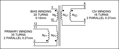
図12. トランスの電気回路図
| Parameter | Conditions | Value |
| Electrical Strength | 50Hz 1 minute, from pins 1–3, 10–12 to pins 5–8 | 1500VRMS |
| Primary Inductance | Pins 1, 12; all windings open. Measure at 275kHz | 120µH ±10% |
| Primary Leakage Inductance | Pins 1, 12; rest of pins shorted. Measure at 275kHz | 3µH (max) |
| Item | Description |
| 1 | Core: EFD15, PC40. Manufacturer: TDK |
| 2 | Bobbin: EFD15 coil former (SMD), 12 pins |
| 3 | Tape: 8.9mm wide insulation tape |
| 3 | Tape: 8.9mm wide insulation tape |
| 3 | Tape: 8.9mm wide insulation tape |
| 4 | Magnet Wire: .25mm diameter with 150°C |
| 5 | Magnet Wire: .27mm diameter with 150°C |
| 6 | Magnet wire: 0.10mm diameter with 150°C |
| 7 | Varnish |
| Note | All wires include insulation |
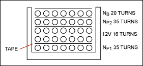
図13. トランスの構造図
| Step | Description |
| Primary NP1 | Start at pin 1. Wind 35 turns of item 4 in approximately 1 layer. Finish on Pin 12 |
| Insulation | Use 1 layer of item 3 for insulation |
| 12V Winding | Start at pins 6 and 5. Wind 16 turns of 2 parallel strands of item 5. Finish at pins 7 and 8 |
| Insulation | Use 1 Layer of Item 3 for Safety Insulation |
| Primary NP2 | Start at pin 2. Wind 35 turns of item 4 in approximately 1 layer. Finish on pin 11 |
| Insulation | Use one layer of item 3 for safety insulation |
| Bias Winding | Start at pin 3. Wind 20 turns of item 6. Spread turns evenly across bobbin. Finish at pin 10 |
| Outer Wrap | Wrap Wwndings with 2 layers of item 3 |
| Final Assembly | Assemble and secure core halves. Varnish impregnate with item 9 |


