Low Noise LT1614 DC/DC Converter Delivers –5V at 200mA from 5V Input
The inverting DC/DC converter function is traditionally realized with a capacitor-based charge pump. Although simple, the output impedances of the best charge pump solutions are in the 5Ω to 10Ω range, resulting in significant regulation issues when the load current increases beyond a few tens of milliamperes. The LT1614 inductor-based inverting DC/DC converter uses closed-loop regulation to obtain an output impedance of 0.1Ω, eliminating output voltage droop under load.
Figure 1 details the 5V to –5V converter circuit. The LT1614 contains an internal 0.6Ω switch rated at 30V, allowing up to 28V differential between input and output. Quiescent current is 1mA and the device contains a low-battery detector with a 200mV reference voltage. The device switches at 600kHz, allowing the use of small, inexpensive external inductors and capacitors. In fact, the total cost of the components specified in Figure 1 (excluding the LT1614) is approximately $0.70 in 10,000-piece quantities.
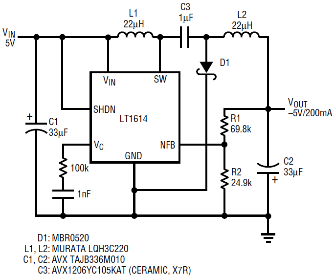
Figure 1. 5V to –5V DC/DC converter uses an inverting topology and delivers 200mA
The LT1614 operates by driving its NFB pin to a voltage of –1.24V, allowing direct regulation of the negative output. This converter topology, which consists of inductors in series with both input and output, results in low output noise and also in low reflected noise on the 5V input supply. The output and switch nodes are shown in Figure 2. Output ripple voltage of 40mV is due to the ESR of the tantalum output capacitor C2. Ripple voltage can be reduced substantially by replacing output capacitor C2 with a 10µF ceramic unit, as pictured in Figure 3.
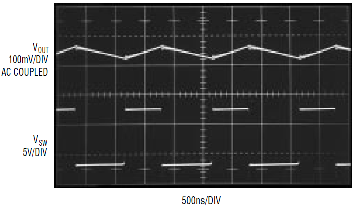
Figure 2. LT1614 output and switch node with a 33µF tantalum capacitor and 200mA load current
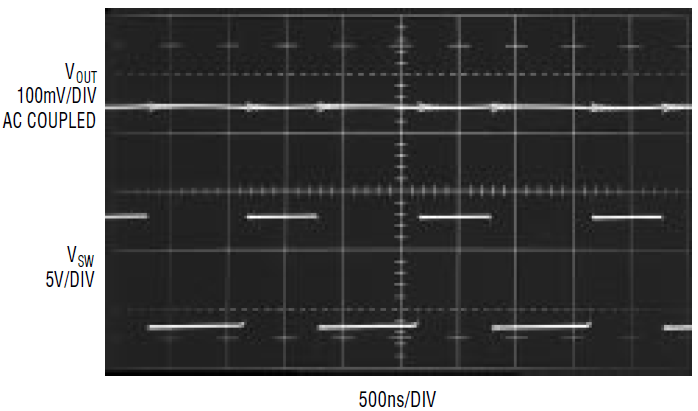
Figure 3. LT1614 output and switch node with a 10µF ceramic output capacitor and 200mA load current
In layout, be sure to tie D1’s cathode directly to the LT1614’s GND pin, as shown in Figure 1. This keeps the switching current loops tight and prevents the introduction of high frequency spikes on the output. The low noise that can be achieved with a ceramic capacitor may be corrupted by noise spikes if proper layout practice is not followed. To illustrate this point, output and switch waveforms from Figure 1’s circuit, with a 10µF ceramic output capacitor and 200mA load, but with D1’s cathode arbitrarily connected to the ground plane, are shown in Figure 4. 60mV switching spikes ruin an otherwise clean output.
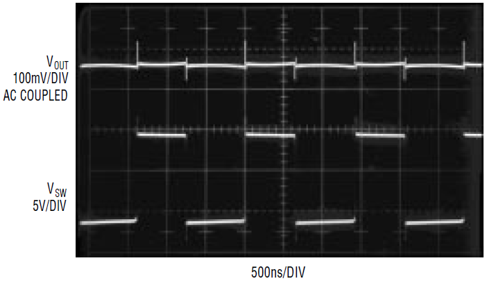
Figure 4. Improper placement of D1’s cathode results in 60mV switching spikes at output, even with a 10µF ceramic output capacitor
Efficiency of the circuit is detailed in Figure 5. Efficiency reaches 73% at a 50mA load, and is above 70% at a 200mA load. Larger inductors with less copper resistance can be used to increase efficiency, although such inductors are more expensive than the Murata units specified.
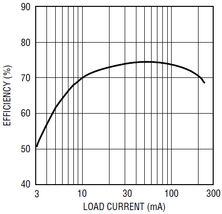
Figure 5. 5V to –5V converter efficiency reaches 73%


