Low Dropout Regulator Can Be Directly Paralleled to Spread The Heat
Introduction
The 3-terminal adjustable linear regulator has been around since 1976, but since then, little has changed in its essential architecture. A 1.2V reference is boosted to generate a regulated output somewhere above a minimum 1.2V. What if, however, you throw away the voltage reference and replace it with a precision current source? The result is a giant leap forward in linear regulator capability, performance and versatility. The LT3080 is the first adjustable linear regulator to do just that. This deceptively simple architectural change allows this new regulator to be directly paralleled to spread the current load and thus spread dissipated heat among the ICs. Spreading the heat makes it possible to use linear regulators in high output current, all-surface-mount applications where only a limited amount of heat can be dissipated in any single spot on a board—applications that previously demanded a switching regulator.
When regulators are surface mounted on a system board, conductive dissipation and air-cooling limits the amount of power that can be dissipated in each chip. With a typical board, allowing a max operating temperature of 60°C to 70°C, a linear regulator can safely dissipate approximately 1W to 2W. This number depends on the ability of the board to spread the heat and airflow across the board. If high power requirements cause the regulator to generate more heat than the board can dissipate, the regulator must be mounted separately on a heat sink. In all-surface-mount systems, this is not an option, so the limitation of power dissipation (1W for example) limits the output current.
Figure 1 shows the maximum output current at different input-output differentials that can be obtained for a regulator with both 1W and 2W dissipation. 2W dissipation is a reasonable limitation on a single regulator. Paralleling LT3080s increases the maximum total output current by spreading the heat, helping to maintain low peak temperatures.
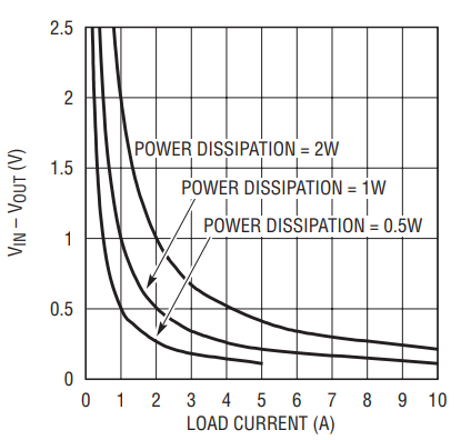
Figure 1. The available output current as a function of input-output differential and allowable power dissipation. At 2W, 1A output currents are possible even with 1V to 2V input-to-output differential.
The LT3080 is also especially well suited to applications needing multiple rails. The new architecture adjusts down to zero with a single resistor, handling modern low voltage digital ICs. Adjusting to zero output makes it possible to shut off the powered circuitry when the input is preregulated—such as a 5V or 3.3V input supply. External resistors in series with IN can help spread the heat, keeping the system all surface mount.
Finally, the new regulator is made in a 40V bipolar process. This allows high input voltage as well low operating voltage, since bipolar transistors turn on at 0.6V.
Internal Precision Current Source Makes it Possible to Parallel the LT3080
A precision “zero” TC 10µA internal current source is connected to the non-inverting input of a power operational amplifier. The power op amp provides a low impedance buffered output from the voltage on the non-inverting input. A single resistor from the non-inverting input to ground sets the output voltage and if this resistor is set to zero, zero output results. As can be seen, any output voltage can be obtained from zero up to the maximum defined by the input power supply.
| LT317 | LT1086 | LT3080 | |
| Dropout (V) | 3V | 1.5V | 1.3V or 300mV |
| Min Load (mA) | 10 | 10 | 0.3 |
| Min Output (V) | 1.2 | 1.2 | 0 |
| IOUT (A) | 1.5 | 1.5 | 1.1 |
| Parallel Operation | — | — | |
| External Resistors | 2 | 2 | 1 |
| Parameter | Value |
| Load Regulation, IOUT = 10mA to 1.1A | <1mV |
| Line Regulation, IN = 2V to 40V | <1mV |
| SET Pin Current | 10µA ±1% |
| Min Load Current | 0.3mA |
| SET to OUTPUT Offset | 1mV |
| Operating Temp Range | –55°C to 125°C |
| Dropout (3-Terminal) 1.1A | 1.3V |
| Dropout (4-Terminal) 1.1A | 0.3V |
| Ripple Rejection (120Hz) | 75 dB |
What is not so obvious from this architecture is the benefits of using a true internal current source as the reference as opposed to the bootstrapped voltage reference of older regulators. A true current source allows the regulator to have gain and frequency response independent of the output voltage since the loop gain does not change. Traditional adjustable regulators, such as the LT1086, have a change in loop gain and bandwidth with output voltage as well as bandwidth changes when the set/adjustment pin is bypassed to ground. With the LT3080, however, the loop gain remains unchanged with changing output voltage or bypassing. Output regulation is no longer fixed at a percentage of the output voltage but rather a fixed number of millivolts. With a true current source, all the gain in the buffer amplifier provides regulation; none of it is needed to amplify the reference to a higher output voltage. This, and the LT3080’s precise DC characteristics, makes it possible to easily parallel regulators (see below: “It is Easy to Parallel the LT3080”).
High Performance
No sacrifices were made in regulator performance for the LT3080. Line and load regulation are excellent over temperature. Its low dropout and a new architecture make it extremely versatile. On chip trimming keeps the accuracy of the reference current below one percent, and the offset voltage between the SET pin and the output to under 2mV.
Line regulation is virtually immeasurable, a few nanoamps, since the internal circuitry double-regulates the current source section. The temperature performance of the reference is shown in Figure 2 and is nearly flat from –55°C to 150°C. Thermal limiting is set at about 160°C. Quiescent current is only about 300µA, allowing this device to be used in light load and battery-powered applications. High frequency ripple rejection is also excellent, making the LT3080 a good fit as a post regulator to switching regulators when low output ripple is needed.
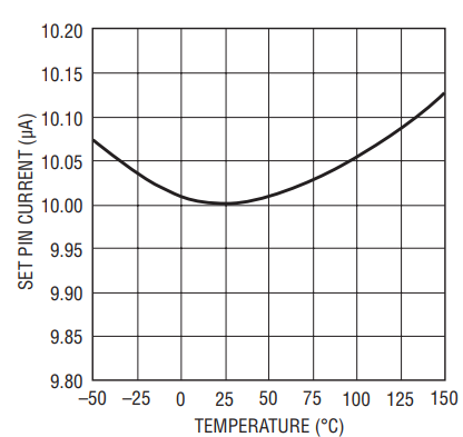
Figure 2. Temperature performance of the LT3080’s precision current source.
Operation of the LT3080
Figure 3 shows a block diagram of the LT3080. The simplest application, as a 3-terminal adjustable regulator, is shown in Figure 4. The VCONTROL and IN pins are tied together. (These two pins can connect to different supplies for additional thermal benefits, described below.) The only added components are input and output capacitors and a resistor to set the output voltage. In this case, the output is set to 1.8V, which at 1.3V dropout works with a 3.3V input. Input and output capacitors are required for stability—they can be ceramic, tantalum, or electrolytic capacitors. Unlike older 3-terminal regulators, the minimum load current is guaranteed at only 1mA for this device. By making the adjustment resistor zero or tying the SET pin to the ground with a switch, the output goes to zero, turning off connected circuitry. Typically, the quiescent current is under 300µA.
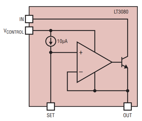
Figure 3. Block diagram of the LT3080. Four terminals are available from the package to allow the device to be used in a low dropout mode with only 300mV input-to-output dropout.
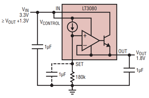
Figure 4. Basic hookup for the LT3080 regulator. The IN and VCONTROL pins are tied together and a single resistor sets the output voltage. A 1µF output capacitor ensures stability. If the adjustment resistor is adjusted to zero, the output is zero.
The SET pin is very high impedance and the output voltage is set by the 10µA current times an external resistor. Even a 0.1µF capacitor is large enough to bypass the SET pin at 60Hz, allowing for reduction of output noise and pickup into the SET pin.
With a capacitor on the SET pin, output noise is 40µVRMS—about the same as many low noise regulators. In other applications, the SET pin can be driven with an amplifier or a reference voltage to be used as a power buffer. With multiple regulators, the SET pins and outputs can be tied together for paralleling the regulator (described below). Grounding the SET pin brings the output to zero.
VCONTROL Pin Offers Additional Ways to Spread the Heat
Clearly, one of the driving design objectives for this new regulator was to enable the thermal design for surface mount boards—notably eliminating the need for heat sinks. Paralleling LT3080s makes a significant difference, but another feature also helps. The collector of the output transistor is available at the VCONTROL pin (see Figure 3). This can decrease peak temperatures in two ways.
First, the dropout on the collector is 400mV (IN pin) so it can take a lower voltage supply than is used for the LT3080’s control circuitry (1.3V dropout). Lowering the input-to-output voltage on the power transistor increases efficiency and thus reduces dissipation.
Second, a resistor can be inserted in series with the collector. Adding this resistor splits power dissipation between the internal power transistor and an external resistor so that some of the heat from the IC can be moved to elsewhere on the PC board. Figure 5 shows such a design using a 2.9Ω resistor. The dropout voltage for the output transistor is only 400mV, so several volts can be dropped across the external resistor, minimizing the heating of the IC. At full load, the external resistor drops approximately 3V and dissipates 3W. To minimize peak temperatures on a PC board, this resistor can be split into several 1Ω resistors and thus further spread dissipated heat. The power dissipation in the LT3080 peaks at about 750mW when the power dissipation in the resistor and the power dissipation in the transistor are equal. The copper planes in the PC board can easily handle this power.
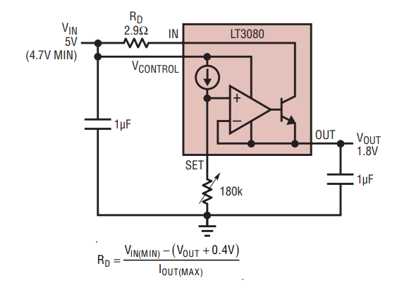
Figure 5. Adding a resistor in series with the collector of the output device to remove some of the power dissipation from the regulator. This disperses heat around the surface mount board rather concentrating it at the regulator.
Of course the LT3080 can be operated in 3-terminal mode by simply connecting the VCONTROL pin to the power input pin, but this limits the input to the 1.3V dropout of the regulator. Alternately, by tying the IN pin to a lower voltage than VCONTROL, it is possible to produce a 1.1A, 2.5V to 1.8V or 1.8V to 1.2V regulator with low dissipation—likewise for other low IN – OUT differentials. To achieve the same peak operating temperatures, the dissipation constrained design current must be lower for higher IN – OUT differentials, such as 5V to 3.3V or 3.3V to 1.5V.
It is Easy to Parallel the LT3080
The architecture of the LT3080 allows direct paralleling unlike any other type of regulator. Parallel linear regulators distribute the current load and distribute power dissipation around the system board. Need more power but can’t afford more spot heating? Add more regulators. Even paralleling 5–10 devices is reasonable.
Practical current sharing by parallel LT3080s is made possible by internal trimming, which keeps the offset voltage between the adjustment pin and the output under 2mV. Figure 6 shows how easy it is to parallel LT3080s. Simply tie the SET pins of the LT3080s together, and do the same for the IN pins. This is the same whether it’s in 3-terminal mode or has a separate IN supply. The outputs are also connected in common but with a small piece of PC trace in series with each OUTPUT pin serving as ballast to equalize the currents. PC trace resistance in milliohms/inch is shown in Table 3. Only a tiny area is needed for ballasting.
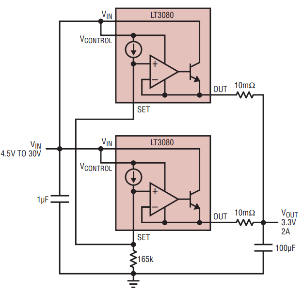
Figure 6. Paralleling of two regulators. Need more current? Add more regulators. Current sharing is assured by the 10mΩ PC board traces, which act as ballast resistors.
| 10mil Width | 20mil Width | |
| 1oz Weight | 54.3 | 27.1 |
| 2oz Weight | 27.1 | 13.6 |
Figure 6 shows two devices with a small 10mΩ ballast resistor, which at full output current gives better than 80% equalized sharing of the current. The external resistance of 10mΩ (5mΩ for the two devices in parallel) only adds about 10mV of output regulation drop at an output of 2A. Even with the 1V output, this only adds 1% to the regulation.
Thermal Performance
Two LT3080 3mm × 3mm QFN devices are mounted on a double sided PC board. They are placed approximately 1.5 inches apart and the board is mounted vertically for convection cooling. Two tests were set up to measure the cooling performance and current sharing of these devices.
The first test was done with approximately 0.7V input-to-output differential and a 1A load per device. This setup produced 700mW dissipation in each device and a 2A output current. The temperature rise above ambient is approximately 28°C and both devices were within ±1°C of each other. Both the thermal and electrical sharing of these devices is excellent. The thermograph in Figure 7 shows the temperature distribution between these devices, where the PC board reaches ambient within about 0.5in from the devices.
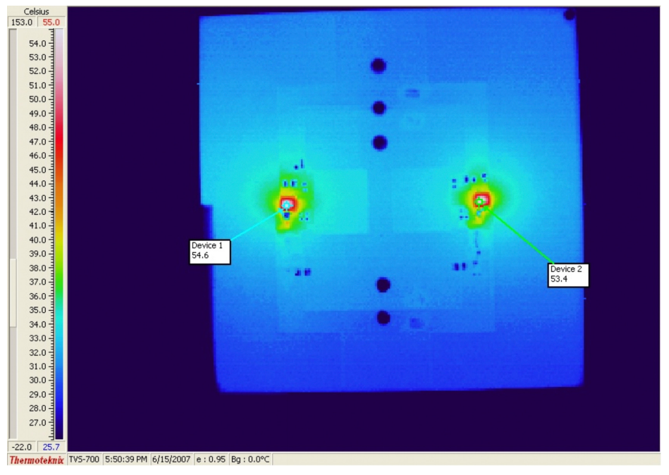
Figure 7. Thermograph shows two regulators, each dissipating 0.7W from a 0.7V input-to-output differential at 2A total load. The result is a 28°C rise over ambient at each IC on a two sided PC board.
Figure 8 shows what happens when the power is increased to 1.7V across each device. This produces 1.7W dissipation in each device and a device temperature of about 90°C, about 65°C above ambient. Again, the temperature matching between the devices is within 2°C, showing excellent tracking between the devices. The board temperature drops to about 40°C within 0.75 inches of each device.
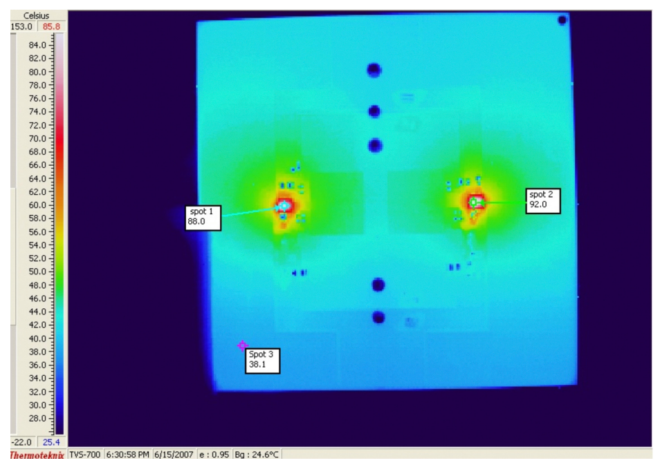
Figure 8. Thermograph shows a 65°C rise for two regulators, each dissipating 1.7W from a 1.7V input-to-output differential at 2A load.
While 95°C is an acceptable operating temperature for these devices, this rise is in a 25°C ambient environment. For higher ambient temperatures, the temperature rise must be controlled to prevent the device temperature from exceeding 125°C. A 3-meter-per-second airflow across the devices decreases the device temperature by about 20°C, providing a margin for higher operating ambient temperatures. Also, this example is for a 2-layer board. A 4-layer board would provide better power dissipation.
Conclusion
The LT3080’s breakthrough design and high performance DC characteristics allows it to be paralleled for high current all-surface-mount applications. It is also adjustable to zero output, an impossible feat with a traditional 3-terminal adjustable linear regulator. It is optimized for new circuit applications and all-surface-mount system assembly techniques—especially high performance, high density circuit boards.


