Low Distortion Rail-to-Rail Amplifiers Drive ADCs and Cables
Introduction
Operating from supplies as low as 2.5V, the 325MHz LT1806 and the 180MHz LT1809 rail-to-rail amplifiers provide the distortion and noise performance required by low voltage signal conditioning and data acquisition systems. Rail-to-rail inputs and outputs allow the entire supply range to be used, and the high output current capability, 60mA typical on a 3V supply, is ideal for cable-driver applications. The LT1806 is optimized for noise and DC performance, featuring a low voltage noise of 3.5nV/√Hz and a maximum offset voltage of 550µV. The LT1809 is optimized for slew rate and distortion, featuring a slew rate of 350V/µs and low harmonic distortion –90dBc at fC = 5MHz (VS = 5V, VO = 2VP-P). Both parts are fully specified for 3V, 5V and ±5V operation and are available in 8-lead SO and 6-lead SOT-23 packages. A shutdown function is included that disables the amplifier and reduces the supply current to less than 1mA.
Performance
Table 1 summarizes the performance of the LT1806 and LT1809. Note that input offset voltage is specified at both the positive and negative supply rails, in contrast to most competitive parts, which are only specified at mid-supply.
| Parameter | LT1806 | LT1809 |
| Gain-Bandwidth Product | 325MHz | 180MHz |
| Slew Rate | 140V/µs | 350V/µs |
| Input Voltage Noise | 3.5nV/√Hz | 16nV/√Hz |
| Harmonic Distortion, RL = 1k fC = 5MHz, VS = 5V, AV = 1, VO = 2VP-P |
–80dBc | –90dBc |
| Settling Time 0.01% VSTEP = 2V, VS = 5V, AV = 1 |
60ns | 40ns |
| Operating Supply Range | 2.5V to 12V | 2.5V to 12V |
| Output Swing High IL = 5mA IL = 25mA |
VS – 0.18V Max VS – 0.7V Max |
VS – 0.16V Max VS – 0.5V Max |
| Output Swing Low IL = 5mA IL = 25mA |
0.13V Max 0.4V Max |
0.08V Max 0.3V Max |
| Short Circuit Current, VS = 3V | ±30mA Min | ±40mA Min |
| Input Offset Voltage VCM = V+ , V– | 0.55mV Max | 2.5mV Max |
| Input Bias Current | 13µA Max | 28µA Max |
| CMRR VS = 5V, VCM = V+ to V– |
80dB Min | 69dB Min |
| PSRR VS = 2.5V to 10V, VCM = 0V |
91dB Min | 73dB Min |
| Supply Current, VS = 5V | 13mA Max | 17mA Max |
| Supply Current, VS = 5V Shutdown | 0.9mA Max | 0.8mA Max |
The distortion vs frequency for the two parts is shown in Figures 1–4. The harmonic distortion was measured with two loads: 100Ω, which is representative of a cable-driving application, and 1kΩ, which is typical of signal-conditioning applications. Both devices are quite good but the LT1809 provides the ultimate in distortion performance.
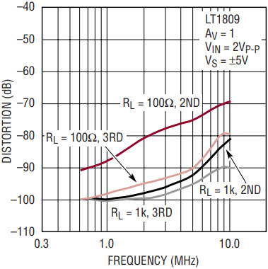
Figure 1. LT1809 distortion vs frequency.
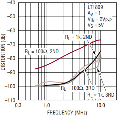
Figure 2. LT1809 distortion vs frequency.
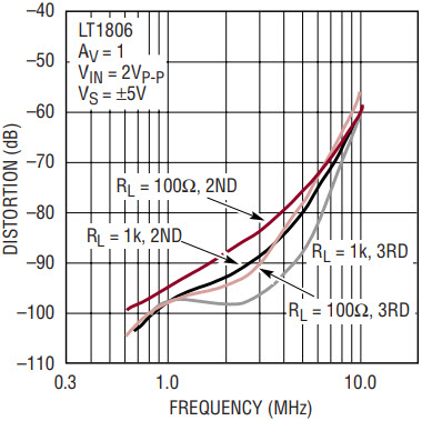
Figure 3. LT1806 distortion vs frequency.
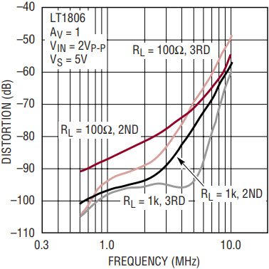
Figure 4. LT1806 distortion vs frequency.
Single 3V Supply, 4MHz, 4th Order Butterworth Filter
A low distortion, low voltage filter, suitable for antialiasing applications, is shown in Figure 5. The filter is a cascade of two inverting 2nd order sections, with values selected to give a Butterworth response. In this configuration, signal swing on the inputs of the op amps is small, resulting in good distortion performance. Distortion was measured at –83dBc at 1MHz, VO = 2.25VP-P. The overall filter response (Figure 6) shows a stopband that has greater than 95dB rejection of frequencies up to 100MHz. Such stopband depth would be difficult to achieve with a dual op amp because of crosstalk and layout issues.
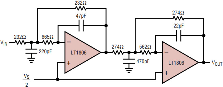
Figure 5. Single 3V supply, 4MHz, 4th order Butterworth filter.
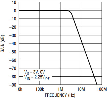
Figure 6. Frequency response of Figure 5’s filter.
Single 5V Supply Video-Cable Driver
The high output current capability of the LT1809 can be put to use in video-cable-driver applications. Figure 7 shows an AC-coupled video driver using a single 5V supply. The input signal is level shifted to half supply by coupling capacitor C1 and resistor divider R1/R2. An AC gain of two in the amplifier, set by resistors R3 and R4 and capacitor C2, compensates for the loss due to the output termination resistors R5 and RLOAD, resulting in an overall gain of one. Figure 8 shows the frequency response of the driver. The –3dB bandwidth is about 95MHz and peaking is less than 1dB.
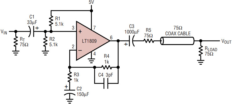
Figure 7. Single-supply video line driver.
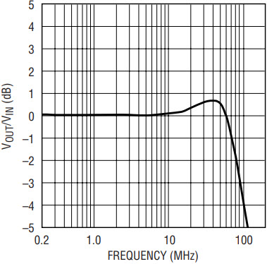
Figure 8. Frequency response of Figure 7’s circuit.
Buffering Data Converters
Driving ADCs is a tricky business. Looking at the circuit of Figure 9, you would correctly surmise that the signal flows from left to right. Entering the noninverting input, this signal takes a gain of 2 in the LT1809. It passes through the 6.8MHz lowpass filter formed by R3 and C1 and is applied to the LTC1420 ADC. With the 10Msps, 12-bit LTC1420 set in a gain of 1 and its internal reference set at 2.048V, the full-scale signal is about 1VP-P, input referred. Figure 10, a 4096 point FFT, shows results achieved with a 1.394MHz signal. The spurious free dynamic range is about 90dB, with performance limited by the ADC’s nonlinearities rather than by the LT1809. (Typical SFDR for the LTC1420 is 83dB.)
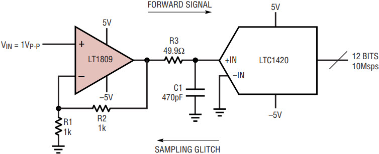
Figure 9. High speed ADC driver.
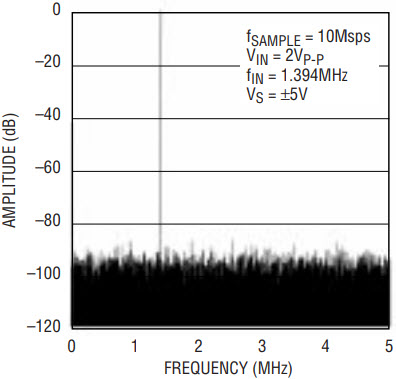
Figure 10. 4096 point FFT of the 12-bit ADC’s output.
However, there is also a signal, the ADC sampling glitch, that travels from right to left. It is caused by a small flying sample capacitor in the ADC front end, which introduces an AC short circuit at the ADC’s input ten million times per second. This signal can cause grief to upstream circuitry unless means are taken to attenuate it. The LT1809 performs admirably in this task. Tracing the reverse signal path from the LTC1420, C1 serves as a storage capacitor and R3 limits the glitch current into the LT1809’s output. The LT1809’s collector output stage incorporates proprietary local feedback to reduce its output impedance (about 20Ω at 100MHz) and this helps attenuate the glitch as well. However, a remnant glitch persists and works its way through R2 and R1, being attenuated by a factor of 2 in the process, and arrives at the LT1809 inverting input. For best performance, the amplitude of the glitch at this point should have been reduced to several millivolts. If it is larger than about 25mV, the rule-of-thumb for BJT differential pairs, the input stage will begin to be driven outside of its linear region and excess distortion will result. The excellent results of Figure 10 indicate that the circuit is not suffering from this effect.
Conclusion
The LT1806 and LT1809 provide complementary solutions for high speed, low voltage signal conditioning. The LT1806, with its low voltage noise of 3.5nV/√Hz and a maximum offset voltage of 550µV, is ideal for applications requiring low noise or DC precision, whereas the LT1809 provides the ultimate in distortion performance. The rail-to-rail inputs and outputs of the devices maximize dynamic range and can simplify designs by eliminating the need for a negative supply. This combination of features in a SOT-23 package makes the devices a top choice for handling the challenges of low voltage signal conditioning.


