要約
Haptic sensing technology, with its ability to render complex tactile experiences, is becoming popular in portable applications. Excessive power dissipation is a concern with current piezo haptic drivers' implementations. Although the piezoelectric actuator represents a capacitive load, considerable power is dissipated to drive it. This design solution reviews the shortcomings of current piezo haptic driver implementations and introduces a novel, regenerative, boost converter-based implementation that minimizes power dissipation, helping maximize the battery life of portables.
Introduction
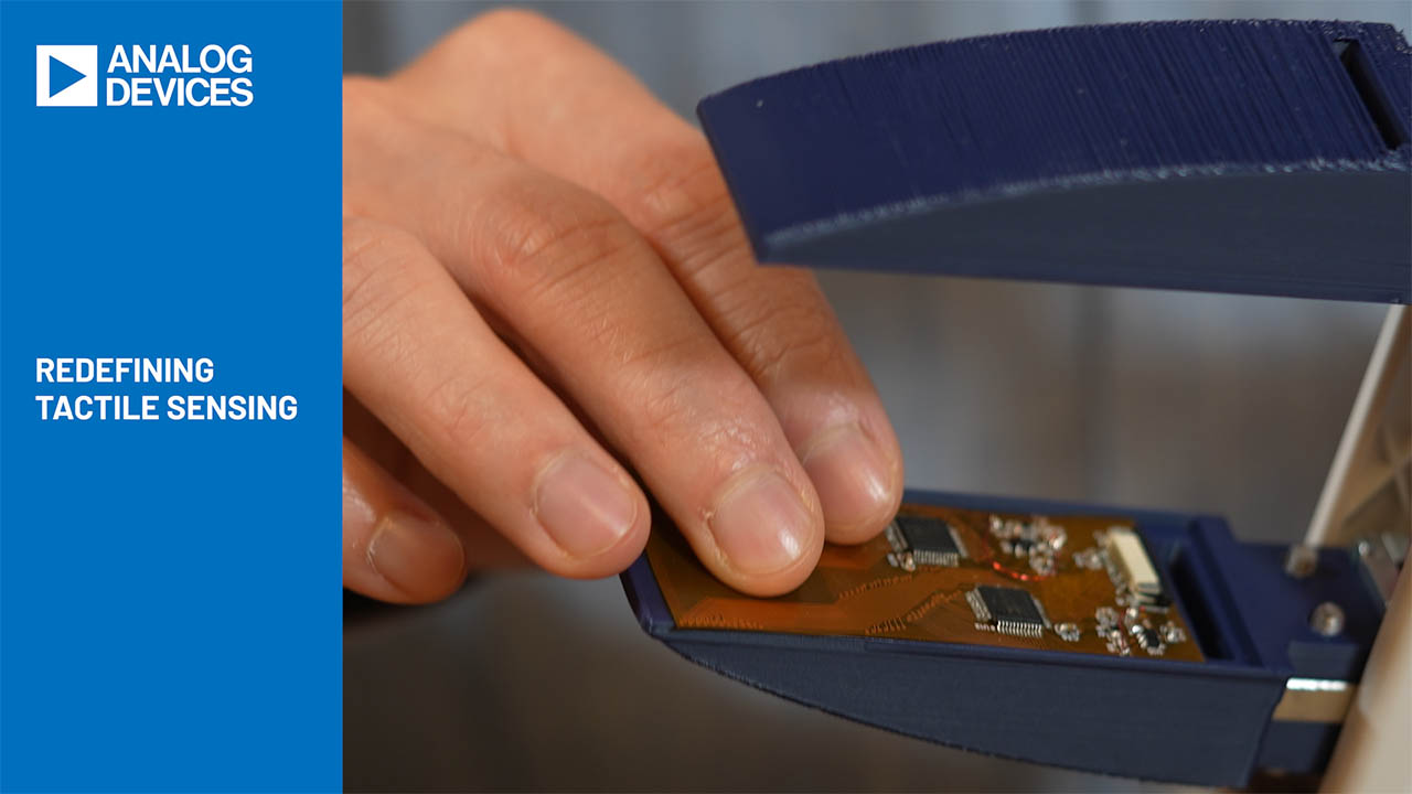
During your last hike you may have taken a picture of a beautiful and wild creature, a snake! Were you tempted to move your fingers over its scales to feel its smooth shape? Before long, you may be able to do just that—without risk of getting bit. With the help of haptics, the tactile feedback technology that exploits the sense of touch by applying forces, vibrations, or motions to the user, is growing by leaps and bounds and will be soon able to render the feeling of the complex textures described above. More mundanely, studies show that, on average, virtual keyboard users will complete typing tasks significantly faster when provided with tactile feedback.
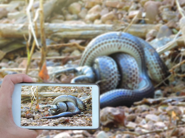 Figure 1. Virtual and safe touch with haptics.
To accomplish this, haptic technology is moving beyond the basic options possible with a vibrating motor and by exploiting the flexibility of piezoelectric actuator technology.
The Piezo Actuator
The piezoelectric actuator converts an electrical signal into a precisely controlled physical displacement. Signals of hundreds of volts at frequencies of a few hundred Hertz are necessary to produce a meaningful displacement (Figure 2). Just as the human ear perceives certain frequency sounds to be louder than others, vibrations are perceived differently upon their intensity. As in the hearing process, the intensity of the tactile experience is proportional to the frequency and amplitude of the vibrating signal. Changing the vibration intensity and pattern creates a virtually limitless number of combinations, rhythms, or messages. When operated below their electrical resonant frequencies, piezo actuators are capacitive in nature. Piezo-based haptics offer several advantages over competing technologies, including fast response time, thin profile, low power, and a wide range of available piezo characteristics and mounting techniques.
 Figure 2. Typical piezo haptic driver waveform.
The Haptic System
Figure 3 shows a high-level block diagram of a multi-channel haptic system. As an example, when the user strikes a key, a capacitive touch sensor IC detects the action and reports the information to the microprocessor, which instructs the piezo haptic driver to apply the appropriate vibration pattern to the piezo element selected with the high-voltage multiplexer. Accordingly, the user receives a physical sensation of having struck the key. Naturally, for this to work the loop response must be faster than the operator detection time lag. A haptic event with a delay of 5ms or less will be perceived by the user as simultaneous.
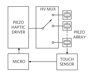 Figure 3. Multi-channel haptic system example.
Typical Solution
Figure 4 shows a typical piezo haptic driver IC implementation for portables. A boost converter steps up the lithium-ion battery voltage to 60V, providing the necessary high-voltage power supply to the Class AB amplifier.
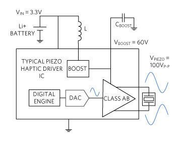 Figure 4.Typical haptic driver solution.
This solution requires significant input power, which is dissipated in the IC. High power dissipation is problematic in portable applications. First, the Class AB linear amplifier is inherently dissipative (say 60% efficiency), and the boost converter adds to the losses with its own finite efficiency (say 85%). As an example, a 1µF capacitance with 100VP-P at 200Hz adds up to a load of 1W:
P = 1/2 CV2f = 0.5 x 10-6 x 1002 x 200 = 1W
With a system efficiency of 50% (085 x 0.6), the input power from the battery adds up to 2W, a power dissipated on the IC.
Ideal Solution
An ideal solution is one that recovers the capacitor energy as opposed to dissipating it. One solution would be to use a Class D amplifier instead of a Class AB one. This way, the amplifier losses are minimized, but the boost converter losses remain. Additionally, a Class D amplifier solution requires a complicated output filter that is bulky and introduces additional losses.
The next step is to combine the amplification and the boost function into one single circuit as shown in Figure 5. Notice that the high voltage, 200Hz waveform is very slow compared to the boost converter clock frequency (approximately 500kHz), resulting in a switching regulator with a slowly varying output. Figure 5 shows also the haptic voltage and current waveforms with their amplitude, sign, and phase relationship. During the positive half-wave period, the inductor current charges the capacitor/piezo. During the negative half-wave, the current is returned to the input capacitor through the rectifying MOSFET transistor T1, conducting reverse current when ON. The result is an energy recycling scheme which yields virtually no losses, except for the these associated with the switching losses and finite RDS(ON) of the MOSFET transistors. Notice how the controller IC is a cost-effective low-voltage device and only the external MOSFETs and passives are high voltage. The capacitor CHV implements the necessary level translation between the low-voltage driver and the high-voltage MOSFET gate.
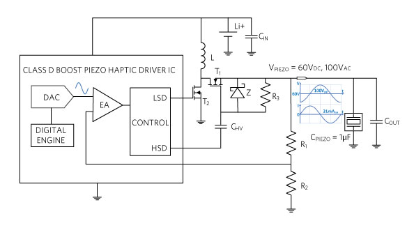 Figure 5. Boost converter regenerative solution.
High-Efficiency Piezo Haptic Actuator Driver
As an example, the MAX77501 is a high-efficiency driver for piezo haptic actuators and is optimized for driving up to 2µF piezo elements. It can generate a single-ended haptic waveform of up to 110VP-P amplitude from a 2.8V to 5.5V input power supply or a single cell Li+ battery. Memory playback (RAM) and real-time streaming (FIFO) of haptic waveforms are supported. A 25MHz SPI interface provides full system access and control, including fault reporting and monitoring. This allows for a rapid 600µs playback startup time from shutdown. The on-board memory can be dynamically allocated as multiple waveform storage or as a FIFO buffer. The IC also implements an ultra-low power boost architecture that provides the lowest power consumption solution for a haptic actuator driver. Built-in undervoltage lockout (UVLO), cycle-by-cycle overcurrent limit, overvoltage and thermal shutdown protections ensure safe operation under abnormal operating conditions. The IC is available in a 30-bump, 0.4mm pitch, wafer-level package (WLP).
Conclusion
Piezoelectric actuators are a key element of modern haptic sensing systems, helping provide tactile feedback to the user who is interacting with an electronic display in battery-operated, hand-held and wearable devices. Typical piezo haptic drivers are complex and power hungry. This design solution reviews a typical implementation, where significant power is dissipated in the Class AB amplifier driving the piezo and in the boost converter generating the high-voltage power supply. Subsequently, it introduces a novel, regenerative implementation in which the boost converter is both the high-voltage source and the amplifier that drives the capacitive piezo element drawing AC current. The boost converter inductor current, when positive, charges the piezo capacitance. When it is negative, the energy is returned to the input capacitor, effectively implementing a regenerative mechanism that minimizes power losses, thereby maximizing portable battery life.
A similar version of this article appeared December 20, 2019 on Electronic Products.

