A Clean 12-Bit, 10Msps ADC
Introduction
As data conversion rates increase, it becomes difficult to find ADCs that have both good dynamic performance and clean linearity. An exception is the LTC1420, a 12-bit ADC that has excellent dynamics and linearity at sampling rates up to 10Msps, making it ideal for communications, scanners and high speed data acquisition. The versatile LTC1420 operates from either single 5V or ±5V supplies, making it easy to interface to single-or dual-supply systems. A programmable on-chip reference and a PGA input circuit give the user a wide selection of input ranges.
LTC1420 Features
- 10Msps sample rate
- Single 5 or ±5V supplies (250mW)
- 0.35LSB INL typical (1LSB max)
- 0.25LSB DNL typical (1LSB max)
- 71dB S/(N+D) and 83dB SFDR at 5MHz input
- 100MHz full-power-bandwidth sampling
- Input programmable gain amplifier
- Out-of-range indicator
- Small package: 28-pin narrow SSOP
Flexible, Yet Easy to Use
The LTC1420 is a complete solution, with an on-chip sample-and-hold, a 12-bit pipelined ADC and a 15ppm programmable reference (Figure 1). The wideband sample-and-hold circuit can sample analog inputs beyond the Nyquist rate up to its 100MHz bandwidth. The sample-and-hold can operate with single-ended inputs or differential inputs with an outstanding CMRR of 75dB. A low impedance, 2.5V reference output is provided (VCM); it can be used as the negative analog input for single-supply applications. The on-chip programmable reference can be set to 2.048V or 4.096V, or turned off so an external reference can be used.
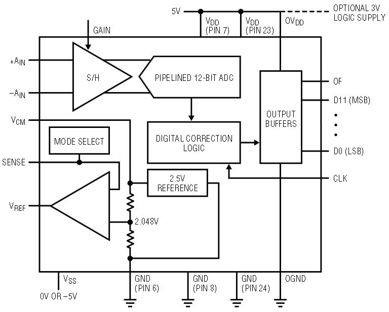
Figure 1. The LTC1420 block diagram shows the 12-bit pipelined ADC core, programmable reference, input PGA and on-chip sample-and-hold.
The LTC1420 has the cleanest linearity of any ADC at this speed. Figure 2 shows typical linearity plots, with better than 0.35LSB INL and 0.25LSB DNL. The INL and DNL errors are guaranteed to be less than 1LSB over temperature for both single supply- and dual-supply applications.
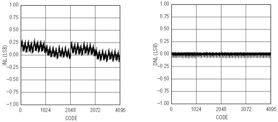
Figure 2. Typical INL (left) and DNL (right) of the LTC1420; the INL/DNL are 0.35LSB/0.25LSB typical and 1LSB max over temperature.
The dynamic performance of the LTC1420 is exceptional, with typical values of 71dB S/(N+D) (signal-to-noise and distortion ratio) and 83dB SFDR (spurious free dynamic range) at Nyquist. The smooth linearity also gives clean dynamic performance with low level input signals, where performance can be degraded by the INL jumps and wobbles found in competitors’ products (Figure 3). Figure 4 shows a 2048-point FFT plot of the LTC1420 with a 5MHz input signal.
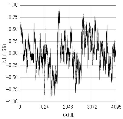
Figure 3. Typical INL for a competitor’s 12-bit, 10Msps ADC; Small input signals near the large jumps and wobbles in the INL will have poor dynamic performance. The clean INL of the LTC1420 prevents this problem.
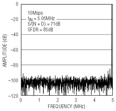
Figure 4. A 2048-point FFT plot of the LTC1420 at 10Msps for a 5.05MHz input signal; the SNR is 71.2dB, SFDR is 85.1dB, THD is –82.4dB and S/(N + D) is 70.9dB.
Single-Supply or Dual-Supply Operation
A single-supply ADC can be cumbersome to work within a dual-supply system. A signal with a common mode of zero volts has to be shifted up to the common mode of the ADC. Shifting the common mode voltage can be accomplished with AC coupling, but DC information is lost. Alternatively, an op amp level shifter can be used but this adds circuit complexity and additional errors. The LTC1420 can operate with dual supplies, allowing direct coupling to the input.
If a single supply is used, the dynamic performance of most ADCs is optimal when the common mode voltage of the input signal is at midsupply (2.5V). To generate this voltage, competitors’ products require an external voltage reference or external resistors and capacitors. The LTC1420 is much easier to use: simply connect AIN– to the 2.5V VCM pin. In dual-supply applications, AIN– can be connected directly to ground. AC coupling signals to the LTC1420 is also easy. All of these modes are shown in Figure 5.
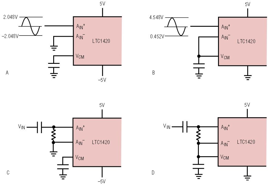
Figure 5. It is simple to directly connect a single-ended signal for a dual-supply (A) or single-supply (B) system (VREF = 4.096V). AC coupling the LTC1420 is also straightforward (C, D).
Programmable On-Chip Reference
The LTC1420 has two reference pins, VCM and VREF, and a reference programming pin, SENSE. VCM is a low impedance 2.5V pin that can be used as the common mode input voltage. The voltage at the VREF pin sets the input span of the ADC to ±VREF/2. If the SENSE pin is connected to VREF or ground, internal circuitry converts the 2.5V reference to either 2.048V or 4.096V at the VREF pin. With a temperature coefficient of 15ppm/°C, both VCM and VREF are suited to serve as the master reference of the system. However, if an external reference is required, tie SENSE to VDD and the on-chip reference amplifier will be turned off and VREF can be directly driven by an external reference.
Pipelined Architecture for High Speed
A/D converters with the cleanest performance are usually made with nonpipelined successive approximation (SAR) based architectures. This is because pipelined converters usually have errors that occur when information is passed from stage to stage in the pipeline. Despite this drawback, pipelining is necessary to obtain high conversion rates. The LTC1420 solves this problem by using a proprietary pipelined architecture that is fast but has accuracy similar to that of slower SAR-type converters. With the LTC1420 you get fast, clean performance without the headache of complicated, time-consuming self-calibration.
Figure 6 shows the timing diagram for the LTC1420. The rising edge of CLK begins a conversion and the digital outputs are updated 70ns later. As with all pipelined ADCs, there is latency in the output data. Output data is updated from the LTC1420 two clock cycles plus 70ns after the input is sampled, so data can be correctly latched on the third rising edge after the conversion starts.
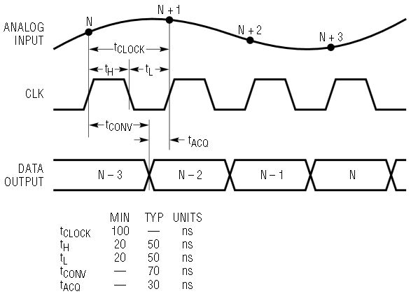
Figure 6. This timing diagram shows two cycles of pipeline delay. The sample is taken on the rising clock edge. Data is available on the third following rising edge.
Easy Interface to 5V or 3V Systems
Another nice feature of the LTC1420 is its dedicated pin for the digital output supply (OVDD). This supply can be set to 5V or 3V, allowing direct interface to 3V systems. Some competitors’ parts support only 5V digital outputs, requiring level-shifting circuitry when interfacing to a 3V system. If 5V digital outputs are desired, OVDD can simply be shorted to VDD to save a bypass capacitor.
Small Footprint
A tiny package and minimal external components make the LTC1420 the smallest 12-bit 10Msps solution on the market. Its 28-pin narrow SSOP package is just 0.09in2, and only four to five 1µF ceramic chip bypass capacitors are needed. Competitors’ parts come in larger packages and can require ten to fifteen bypass capacitors, resistor dividers, external voltage references and op amp level shifters.
Conclusion
The LTC1420 is a simple, flexible 12-bit 10Msps ADC that is easy to use. It has the clean linearity and dynamic performance of a SAR-type ADC at the conversion speed of a pipelined converter. With its high performance and tiny footprint, it is a clear solution for high speed data acquisition.


