The Addition of Active Electron Beam Probing Techniques to an Existing Failure Analysis Process
The Addition of Active Electron Beam Probing Techniques to an Existing Failure Analysis Process
2014年10月17日
Abstract:
As Integrated Circuits (ICs) continue to increase in complexity, the ability to use additional established and effective failure analysis skills becomes significant. Active electron beam probing methods are proven microelectronic failure analysis practices that may be applied with a properly configured Scanning Electron Microscope (SEM). Resistive Contrast Imaging (RCI) and Electron Beam Induced Current (EBIC) are examined and successfully applied as failure site isolation techniques in an existing failure analysis laboratory. The results obtained from these techniques are supported through other failure analysis methods such as optical microscope and curve trace analysis. Ultimately, this paper demonstrates the impact of electron beam probing techniques on enhancing the depth of a present failure analysis process.
I. Introduction and background
Scanning electron microscope
The scanning electron microscope (SEM) is a standard tool in microelectronics and provides a multitude of applications for failure analysis. The SEM generates electrons from its cathode and accelerate them with an electron gun. The potential difference between the cathode and anode of the electron gun determines the acceleration of the electrons. The electron energy generated is measured in electron volts (eV).1 Primarily, the conventional use for the SEM resides in surface topography imaging. Secondary Electrons (SE) provides a high resolution, large depth of field image.2 The SE configuration is the most common mode used for the scanning electron microscope. Additional configurations such as Backscatter Electron (BSE) Imaging and Energy Dispersive X-ray (EDX) use backscattered electrons and x-ray emission respectively to perform varying levels of elemental analysis at and below the surface of the sample.2,3 The SE, BSE, and EDX techniques alone classify the SEM as a cornerstone tool in the failure analysis laboratory.
Active electron beam probing analysis
In addition to the previously discussed SEM modes, other unique configurations can be employed with the SEM to provide added failure analysis capabilities. Active electron beam probing allows isolation of a failure without a detailed understanding of the integrated circuit. This set of techniques capitalize on the ability of the SEM's beam energy to interact with an integrated circuit and the information from this interaction can be analyzed.4 Electron Beam Induced Current (EBIC) and Resistive Contrast Imaging (RCI) are two active electron beam probing methods that can localize failures in the diffusion or conduction layer of the integrated circuit respectively. The primary difference between RCI and EBIC is the acceleration voltage (beam energy). Since it is possible to adjust the penetration depth with the beam energy (1-30 KeV) to a desired analysis level, the RCI or the EBIC effect can be achieved.4 Simply, the beam energy required for penetration to the shallow conduction layer (RCI) is much lower than the beam energy needed for penetration to the deeper diffusion layer (EBIC).
Electron Beam Induced Current (EBIC)
The equipment necessary to perform EBIC imaging is a scanning electron microscope, current amplifier, and an electrical vacuum feedthrough. The only sample preparation is the delid/ decapsulation of the device package.3 An advantage of EBIC over some other active beam probing techniques is the passivation layer does not need to be removed for analysis. Furthermore, no electrical power supply is necessary since the device under test utilizes the beam energy for the current necessary to provide a signal.3 During EBIC analysis, the injected electrons from the electron beam unbalance the equilibrium of the semiconductor and electron/ hole pairs are created. Within the depletion region, the natural field removes excess charge, creating increased reversed bias current. As a result, EBIC signals are generated primarily from buried diffusions (transistors and diodes).5 Measurements can be performed without damage to the surface of the integrated circuit. SEM monitor images can be formed from this effect by amplifying the currents or voltages created by the electron beam.
EBIC limitations
EBIC is a valuable a technique for the evaluation of bipolar semiconductor devices. However, EBIC analysis is limited in the evaluation of MOS technology. The gate oxide sensitivity to primary electron injection is the limiting design factor. The creation of electron/ hole pairs lead to insulators charging causing trapped charges. The effect can result in parasitic MOS transistors or electrostatic discharge damage (ESD). Depending on the electron energy dose to the oxide, the damage can range from an increase in IC leakage current to total failure of the transistor.4
Another EBIC limitation arises as the complexity of the IC increases. EBIC becomes more difficult as the junction depth increases and the complexity of the structures increases.2 This is where a counterpart technique to EBIC known as Optical Beam Induced Current (OBIC) may prove superior. OBIC utilizes a scanning optical microscope (SOM) and can analyze an integrated circuit through the backside due to its IR characteristics.4 Continued evolution and complexity of integrated circuits will continue to increase the value of techniques such as OBIC.
Resistive contrast imaging (RCI)
Similar to EBIC, RCI uses the SEM to generate a resistance image between two nodes of a passivated device. Unlike EBIC imaging, the primary electrons reach only to the conductor level and not the transistor level by using lower beam energy. However, beam energy for RCI must be substantial enough to inject electrons into the conductor level of the device.
To obtain RCI information the primary electron beam energy is increased until the tip of the beam's energy reaches the conductor layer of interest. Usually for RCI, the power and ground inputs are used as test nodes because of their commonality across the integrated circuit. Typically, the ground terminal is grounded and the Vcc terminal is attached to the current amplifier. The technique passes the signal (na) to a current amplifier and the output is displayed on the SEM monitor. The resulting image can potentially show opens or shorts in the metal layer. If a resistance change occurs along a conductor relative to the test lead combination selected (open conductor), the RCI image will display an abrupt contrast change at the open site.3-5 RCI is primarily used to examine metal, polysilicon, and metal to silicon test structures and thin film resistor conductor patterns.3
Only resistance changes relative to the nodes connected to the input of the RCI current amplifier are displayed. Proper node selection is required and conductors without direct paths to output pins cannot be tested. Therefore, RCI use on integrated circuits may be limited and can be difficult to interpret.3,4 However, electrical testing such as ATE or curve trace analysis can determine the most advantageous node connection for RCI and help to minimize this disadvantage.
II. System set up
The Scanning Electron Microscope used for this work is a Hitachi Model S-2700. It is equipped with a Hitachi S6548 current amplifier with gain and noise suppression control. The specimen chamber is configured with a 24 pin electrical vacuum feedthrough. The SEM was recently installed in June of 2001. The first active beam probing analysis experiments were conducted in September 2001.

Figure 1: Specimen chamber of the SEM used for the EBIC and RCI analysis.

Figure 2: The SEM is equipped with a Hitachi S6548 current amplifier.
External grounded sample package leads are connected to the specimen stage using a conductive silver paste. Once the paste is applied, the stage and specimen are baked to solidify the ground connections to the stage. All other leads on the device to be analyzed are bent upward (in the case of a DIP package) and left floating. It is recognized a stage equipped with a properly configured test socket can also be used instead of the more destructive direct connection method described above.
A wire lead is then soldered to a pin of interest such as Vcc and will eventually be connected to the electrical feedthrough. The electrical feedthrough ultimately connects to the current amplifier and the resulting signal is displayed on the auxiliary 1 output of the SEM monitor.

Figure 3: A control unit and a failed unit are set up in the SEM for RCI.
When placing the sample in the SEM, the entire specimen chamber must be brought to room pressure in order to be able to connect the soldered wire lead of the sample to the electrical feedthrough.
The wire connection to the vacuum feedthrough is checked for continuity and the specimen chamber is pumped down to begin the analysis. The wait time for pump down to high vacuum is approximately 8 minutes.

Figure 4: Simplified representation of the RCI and EBIC imaging set up.
The slow scan display mode is necessary for running EBIC and RCI.In TV (fast scan) mode the images appear blurred (20 ms).7 This is because of the slow response output of the RCI or EBIC signal. Navigation issues are overcome by setting one monitor display to SE mode and setting the 2nd monitor to the current amplifier output (Aux 1). Switching quickly to fast scan in combination with SE mode provide a real time image needed to navigate to the area of interest.
III. RCI results
In order to examine the capability of RCI, a 12 bit digital to analog converter (DAC) utilizing bipolar npn transistor technology with a 40 MHz multiplying bandwidth was used. The unit was delided and the digital +Vs input, digital -Vs inputs, and digital ground were located.
A cut was created on the digital +Vs metal trace directly before the input to bit 1 (MSB). The open was created using a Karl Suss probe station equipped with a laser for removing passivation or cutting metal traces. The results of the cut were verified using an optical microscope, SEM (SE), and curve trace analysis.

Figure 5: Optical micrograph of the open created on digital +Vs.

Figure 6: SEM micrograph of the open created on digital +Vs.

Figure 7: Curve trace analysis confirms the change in electrical characteristics created by the intentional cut created on the
+Vs trace (Red: control).
The digital ground lead and the digital -Vs were connected to the stage with silver paste for sample preparation for RCI. The unit and stage were baked for 10 minutes in a 125C oven. A wire lead was soldered to the +Vs input pin. With the stage in place in the SEM, the digital +Vs wire lead was connected to the electrical vacuum feed through. For RCI, the SEM accelerating voltage was reduced to 12kV.
The resulting set up and analysis clearly identified a dark trace originating from the Vs bond pad and terminating at the cut before bit 1. It is clear that RCI quickly and clearly identified a resistance change (open) in the metal trace. Once set up in the SEM, the time needed to identify the open was approximately 3 minutes.

Figure 8: SEM micrograph of the open using the RCI configuration. The open is clearly identified with the abrupt ending of the dark metal trace.

Figure 9: The control unit used for RCI shows the continuation of the +Vs supply path. As a result, no open is identified.
IV. EBIC results
A second 12 bit 40MHZ bipolar DAC was used to examine the capabilities of EBIC. In this case the input to bit 1 was given 3 successive 4000 V ESD pulses. Verification of the electrical damage created was confirmed using curve trace analysis on the bit 1 (MSB) input.

Figure 10: Curve trace analysis confirms electrical damage to bit 1 after receiving 3 successive 4000V ESD pulses. (Red: Control)
After deliding the sample, optical microscope analysis and SEM analysis could not confirm any visual damage.

Figure 11: Optical microscope examination could not confirm visual damage created by the ESD pulse.

Figure 12: SEM (SE) mode of examination could not confirm visual damage created by the ESD pulse.
For the EBIC preparation, the digital ground lead and both digital –Vs leads were connected to the stage with silver paste. The unit and stage were baked for 10 minutes in a 125C oven. Next, a wire lead was soldered to the +Vs input pin. With the stage in place in the SEM, the +Vs wire lead was connected to the electrical vacuum feedthrough.
For the EBIC system configuration, the SEM accelerating voltage was increased to 30 kV in order for the electron beam to be able to penetrate to the diffusion level of the specimen.
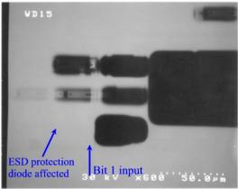
Examination of the Bit 1 transistor area determines one of the structures in the area of interest is not absorbing current.

Figure 13: EBIC output displays a difference in the bit 1 input when compared with the remaining 11 bits. Bit 1 shows absence of a structure.
All other (11 remaining) input bit structures displays a structure that was absorbing beam current. Upon examination of the die plot and schematic for this device, it was determined the missing structure was an ESD suppression diode tied to the bit 1 (MSB) input. As a result of EBIC analysis, the exact defective structure could be identified. Once the examination began in the SEM, the total time to identify the damaged structure was 10-12 minutes.

Figure 14: All other input bits (including bit 2, left) show an additional structure that is not present in the input bit 1 area (bit 1, right).
Incorporation into the current FA process and future work.
The results presented in the previous section were the first successful RCI and EBIC images produced by this failure analysis laboratory. The ability to add a new dimension to the existing failure analysis process poses an exciting opportunity. RCI and EBIC will be integrated into the current failure analysis process as a global fault isolation technique. The techniques main role in the process will be to further isolate the findings of a curve trace analysis. By adding RCI and EBIC to the failure analysis protocol, the ability to localize an electrical anomaly down to the specific structure is increased. Furthermore, curve trace analysis data may not be necessary in certain cases if ATE data or failure analysis history provide enough information to narrow the scope of the failure for proper lead connection.

Figure 15: The addition of EBIC and RCI and the eventual addition of VC can play a significant role in increasing the depth of the current failure analysis tool mix.
The next step in the incorporation of RCI and EBIC is to examine their effectiveness for ESD testing failures. Integrated circuits in the first silicon phase undergo extensive ESD testing before release. In situations where ESD tests are not meeting the design criteria, the ICs may be a candidate to be examined with EBIC or RCI for root cause. Successful and quick root cause isolation can save valuable time during the release process.
The majority of failure analysis done by this laboratory is with multi-chip module technology. With successful RCI and EBIC results established, future work will focus on applications for MCMs. Potential applications identified may be analysis of wire bonds failures, MCM substrate opens, and incoming integrated circuit analysis. Also, future work will also examine the limitations of EBIC on MOS integrated circuit technology.
Voltage Contrast (VC)
The next step in the development process will focus on another active beam probing technique known as voltage contrast (VC). Voltage contrast imaging creates an image in which the degree of contrast is mostly determined by the static voltages of the device. Through brightness analysis, the logic levels of a digital device can be determined. As a result, the voltage on internal circuit nodes can be determined. However, on passivated surfaces, charging from poor beam penetration may occur. Due to this effect, depassivation is usually recommended.3,5 In light of this, future device candidates for the evaluation of VC will take into account the ease of decapsulation and depassivation.
Another specific application of interest with voltage contrast will be in the examination of cross-sectioned capacitors. Voltage contrast can create a contrast pattern to help distinguish a good capacitor from a defective one.6
Charge-Induced Voltage Alteration (CIVA)
Also of future interest is a technique known as Charge-Induced Voltage Alteration (CIVA). The image is generated through measuring the voltage change in a constant current power supply while the device is biased.
As electrons are supplied to good conductors the additional current (na) is absorbed and the result produces practically no change in the supply voltage. In a failing conductor, the voltage change of the conductor becomes measurable. As a result, CIVA is an excellent technique for the analysis of open conductors. The only additional equipment CIVA requires over RCI or EBIC is a constant current source. As with RCI and EBIC, depassivation of the device is not needed.2,4 CIVA's similarities to EBIC and RCI logically make CIVA the next active electron beam probing method to analyze.
VI. Conclusion
Active electron beam probing methods are proven microelectronic failure analysis practices that may be applied with the use of a properly configured Scanning Electron Microscope (SEM). Resistive contrast imaging (RCI) technique was successfully applied to find an open conductor on an IC. Electron Beam Induced Current (EBIC) was also successfully applied to find a damaged ESD protection diode on an integrated circuit. The addition of RCI and EBIC to an existing process provides new depth to this failure analysis tool section mix. Future work will continue to focus on new applications for RCI and EBIC. Additional active electron beam probing techniques such as Voltage Contrast (VC) and Charge-Induced Voltage Alteration (CIVA) will be examined in future work as well.


