
MAXREFDES1151


製品概要
設計リソース
説明
Supercapacitors, by their very name, provide unique benefits in modern electronics. One critical application of supercapacitors is dv/dt suppression. In the dv/dt suppression application, a battery's internal resistance creates a voltage drop at the output of the battery when a load is connected, usually a heavy load. For example, when a 10A load is connected to a 10V battery with an internal resistance of 0.2Ω, the voltage drop is 2V. As the current increases, the battery output voltage decreases, called dv/dt. In order to avoid loss of voltage, designers can opt to design a very large battery into their system. Another more elegant choice is to use a supercapacitor for dv/dt suppression, where the supercapacitor provides additional energy, suppressing the load transient and preventing the battery voltage from collapsing. Such a design allows for a smaller battery, momentary heavy load conditions, and prolonged battery life.
This design includes two parts, the first part uses the MAX406 to charge the supercapacitors with 1A constant current; the second part uses the MAX1725 and MAX985 to realize dv/dt suppression.
The MAX406 is a single, low-voltage, micropower, precision op amp designed for battery-operated systems. It features a supply current of less than 1.2μA that is relatively constant over the entire supply range, which represents a 15 to 20 times improvement over industry-standard micropower op amps. A unique output stage enables this op amp to operate at ultra-low supply current while maintaining linearity under loaded conditions. In addition, the output is capable of sourcing 1.8mA when powered by a 9V battery.
機能と利点
- +2.5V to +10V Single-Supply Range
- 500μV Max Offset Voltage (MAX406A)
- < 0.1pA Typical Input-Bias Current
- Output Swings Rail-to-Rail
- Input Voltage Range Including Negative Remote Alarm Notification (RAI)
詳細
Supercapacitors, by their very name, provide unique benefits in modern electronics. One critical application of supercapacitors is dv/dt suppression. In the dv/dt suppression application, a battery's internal resistance creates a voltage drop at the output of the battery when a load is connected, usually a heavy load. For example, when a 10A load is connected to a 10V battery with an internal resistance of 0.2Ω, the voltage drop is 2V. As the current increases, the battery output voltage decreases, called dv/dt. In order to avoid loss of voltage, designers can opt to design a very large battery into their system. Another more elegant choice is to use a supercapacitor for dv/dt suppression, where the supercapacitor provides additional energy, suppressing the load transient and preventing the battery voltage from collapsing. Such a design allows for a smaller battery, momentary heavy load conditions, and prolonged battery life.
This design includes two parts, the first part uses the MAX406 to charge the supercapacitors with 1A constant current; the second part uses the MAX1725 and MAX985 to realize dv/dt suppression.
The MAX406 is a single, low-voltage, micropower, precision op amp designed for battery-operated systems. It features a supply current of less than 1.2µA that is relatively constant over the entire supply range, which represents a 15 to 20 times improvement over industry-standard micropower op amps. A unique output stage enables this op amp to operate at ultra-low supply current while maintaining linearity under loaded conditions. In addition, the output is capable of sourcing 1.8mA when powered by a 9V battery.
Other features include:
- +2.5V to +10V Single-Supply Range
- 500µV Max Offset Voltage (MAX406A)
- <0.1pA Typical Input-Bias Current
- Output Swings Rail-to-Rail
- Input Voltage Range Including Negative Remote Alarm Notification (RAI)
The MAX1725 is an ultra-low supply current, low-dropout linear regulator intended for low-power applications that demand the longest possible battery life. Unlike inferior PNP-based designs, the MAX1725 PMOS pass elements maintain an ultra-low 2µA supply current throughout their entire operating range and in dropout. Despite its ultralow power consumption, the MAX1725 has tight output accuracy (1.5%) and requires only 1µF output capacitance to achieve good load-transient response.
The MAX985 single micropower comparator features low-voltage operation and rail-to-rail input and output. It has an operating voltage range from 2.5V to 5.5V, making it ideal for both 3V and 5V systems. This comparator also operates with ±1.25V to ±2.75V dual supplies. It consumes only 11µA of supply current while achieving a 300ns propagation delay.
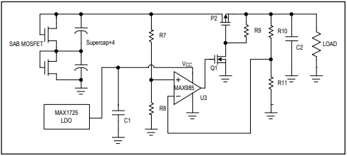
A single, low-voltage, micropower, precision op amp (MAX406), a Zener diode and a current-sense resistor are used to limit the supercapacitor charge current to 1A. A micropower, low-voltage, rail-to-rail I/O comparator (MAX985) and two MOSFETs are used to supply the load when the voltage at the load is lower than the supercapacitor voltage.
An overview of the design specification is shown in Table 1 below.
| Parameter | Symbol | Min | Max |
| Battery Voltage | VIN | 5.5V | 10V |
| Supercapacitor Charge Current | ICHG | 1A | |
| dv/dt when Load Transient (< 5A) Occurs for 500ms (min) | dv/dt | 0 | 10% |
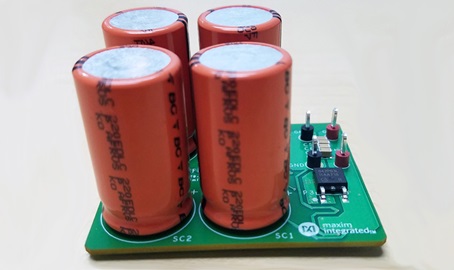
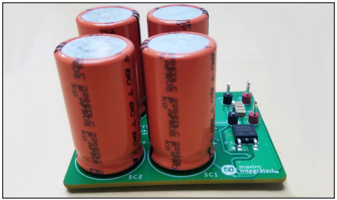
This reference design describes the hardware shown in Figure 1 below. It provides a detailed systematic technical guide to design the dv/dt suppression circuit. The circuit has been built and tested, details of which follow later in this document.
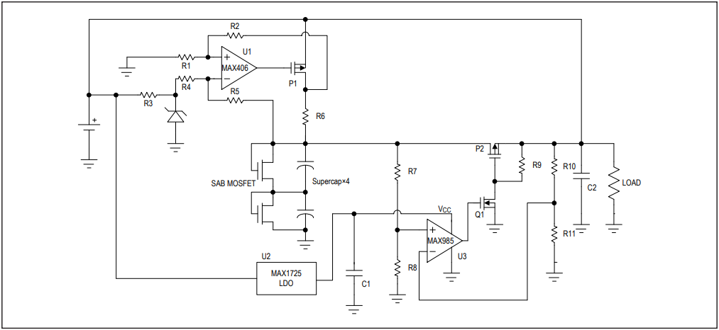
The MAXREFDES1151 uses the supercapacitors to boost the current when a large load transient occurs. This design is for high-voltage input applications. See Figure 2 for the block diagram of this design. The supercapacitor charging current defaults to 1A, and can be adjusted by the current limiter (MAX406 + Zener diode + MOSFET + sensing resistor). The MAX985 and the two MOSFETs act as an ideal diode that turns on when the voltage at the load is lower than the supercapacitor voltage. C2 capacitance needs to be big enough to slow down the voltage drop at the load until the ideal diode turns on. The MAX1725 and C1 provide stable supply voltage to the MAX985 during load transient. Battery input voltage ranges from 5.5V to 10V due to the input voltage range of MAX406 and the rated voltage of the supercapacitors. This solution prevents the power rail from falling over 10% from its original voltage when the load transient (< 5A) occurs for at least 500ms.
Design Procedure for the Supercapacitor dv/dt Suppression Circuit
The supercapacitor dv/dt suppression circuit design process can be divided into two stages: constant charging stage design and dv/dt suppression circuit design.
The following design parameters are used to illustrate the two stages:
- VBAT = Battery Voltage
- VU1IN+ = Noninverting Input of U1
- VU1IN- = Inverting Input of U1
- VU3IN+ = Noninverting Input of U3
- VU3IN- = Inverting Input of U3
Step 1: Designing the Supercapacitor Constant Charging Circuit
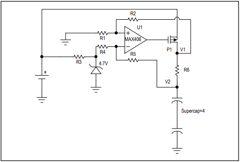
The MAX406, a pMOSFET, a Zener diode, and a resistor are used to control the supercapacitor charging current. Figure 3 is the supercapacitor constant charging circuit. If the supercapacitor charging current is constant, the voltage drop on R6 should not change. The op amp MAX406 and the pMOSFET can control the voltage drop on R6 not to change. In this design, the constant charging current is 1A and R6 is 0.1Ω, so the voltage drop on R6 is 0.1V. If the voltage drop is higher than 0.1V, the MAX406 turns off the pMOSFET and the charging current decreases until the R6 voltage drop become 0.1V; if the voltage drop is lower than 0.1V, the MAX406 turns on the pMOSFET and the charging current increases until the R6 voltage drop becomes 0.1V.
Below is the calculation of R1, R2, R4 and R5 in Figure 3. For an op amp, the noninverting input voltage equals the inverting input voltage, and there's no current flow in the noninverting input and inverting input.
- The noninverting input voltage equals the inverting input voltage:

- The current flows through R1 equal the current flows through R2,

- The current flows through R4 equal the current flows through R5,

From the above three equations we could conclude:

As mentioned, the supercapacitors charging current is 1A, the current sense resistor is 0.1Ω, so the voltage drop on the sense resistor is 0.1V:

To simplify the calculation, assume R1 = R4, R2 = R5:

Choose R5 to be 10kΩ, so R4 = 470kΩ; therefore, R2 = 10kΩ and R1 = 470kΩ.
Step 2: dv/dt Suppression Circuit Design
The ultra-low-IQ, low-dropout linear regulators (MAX1725), the single micropower comparator (MAX985), one nMOSFET, one pMOSFET and four supercapacitors consist of the dv/dt suppression circuit. Figure 4 is the dv/dt suppression circuit block diagram. The MAX1725 is used to supply the comparator MAX985. The MAX985 is used to control the on/off of the nMOSFET. During normal operation, the supercapacitor voltage is equal to the load voltage, so the MAX985 outputs a low voltage and the nMOSFET is off; therefore, the Gate voltage of the pMOSFET is high and the pMOSFET is off, too. The supercapacitor does not supply the load during this period. But when there is a load transient, the load voltage falls below the supercapacitor voltage due to the battery internal resistance, the MAX985 outputs a high level voltage to the Gate of the nMOSFET and the nMOSFET is on, so the Gate voltage of the pMOSFET is pulled low and the pMOSFET is on, then the supercapacitor supplies the load to realize dv/dt suppression.
関連資料
-
MAXREFDES1151 Design Files2021/02/16ZIP2 M
サポートおよびトレーニング
技術的なご質問についての回答は、ナレッジベースを検索してください。また、アナログ・デバイセズのアプリケーション・エンジニアの専任チームが、技術的なご質問にお答えいたします。