MAXREFDES1006

製品概要
設計リソース
説明
The MAX15112 high-efficiency, current-mode step-down regulator with integrated power switches operates from 2.7V to 5.5V and delivers up to 12A of output current in a small 2mm × 3mm package. The MAX15112 offers excellent efficiency with skip mode capability at light-load conditions, yet provides unmatched efficiency under heavy load conditions. The combination of small size and high efficiency makes this device suitable for both portable and nonportable applications.
The MAX15112 uses a current-mode control architecture with a high-gain transconductance error amplifier, which allows a simple compensation scheme and enables a cycle-by-cycle current limit with fast response to line and load transients. A factory-trimmed switching frequency of 1MHz (PWM operation) allows for a compact, all-ceramic capacitor design.
Integrated switches with low on-resistance ensure high efficiency at heavy loads while minimizing critical inductances.
A current-mode synchronous buck is demonstrated using the MAX15112 for a 0.68V DC output application. The power supply delivers up to 4A at 0.68V.
機能と利点
- ±1% Feedback Accuracy Over Load, Line, and Temperature
- Input Undervoltage Lockout
- Programmable Soft-Start
- Adjustable Soft-Start
- External Reference Input
- Selectable Skip Mode Option for Improved Efficiency at Light Loads
使用されている製品
詳細
The MAX15112 high-efficiency, current-mode step-down regulator with integrated power switches operates from 2.7V to 5.5V and delivers up to 12A of output current in a small 2mm x 3mm package. The MAX15112 offers excellent efficiency with skip mode capability at lightload conditions, yet provides unmatched efficiency under heavy load conditions. The combination of small size and high efficiency makes this device suitable for both portable and nonportable applications.
The MAX15112 uses a current-mode control architecture with a high-gain transconductance error amplifier, which allows a simple compensation scheme and enables a cycle-by-cycle current limit with fast response to line and load transients. A factory-trimmed switching frequency of 1MHz (PWM operation) allows for a compact, all-ceramic capacitor design.
Integrated switches with low on-resistance ensure high efficiency at heavy loads while minimizing critical inductances.
Other features include the following:
- ±1% Feedback Accuracy Over Load, Line, and Temperature
- Input Undervoltage Lockout
- Programmable Soft-Start
- Adjustable Soft-Start
- External Reference Input
- Selectable Skip Mode Option for Improved Efficiency at Light Loads
A current-mode synchronous buck is demonstrated using the MAX15112 for a 0.68V DC output application. The power supply delivers up to 4A at 0.68V. Table 1 shows an overview of the design specification.
| PARAMETER | SYMBOL | MIN | MAX |
| Input Voltage | VIN | 2.7V | 4.5V |
| Frequency | fSW | 1MHz | |
| Efficiency | η | 86% | |
| Output Voltage | VOUT | 0.68V | |
| Output Voltage Ripple | ∆VOUT | 20mV | |
| Output Current | IOUT | 0A | 4A |
| Output Power | POUT | 2.7W | |
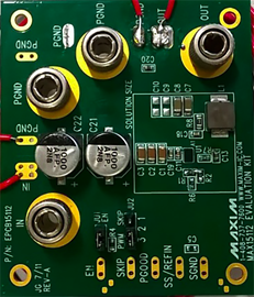
This document describes the hardware shown in Figure 1. It provides a detailed systematic technical guide to designing a synchronous buck using Maxim’s MAX15112 current-mode controller. The power supply has been built and tested, details of which follow later in this document.


Note: The MAXREFDES1006 uses the same board and PCB layout as the MAX15112 EV kit (MAX15112EVKIT).
Synchronous buck converters, as opposed to conventional buck converters, can achieve high efficiency in today’s low-voltage, high-current applications because they replace the catch diode of buck converters with a MOSFET. As a result, the power they dissipate in the off-period is reduced significantly.
In steady state, the low-side MOSFET is driven such that it is complementary with respect to the high-side MOSFET. This means whenever one of these switches is on, the other is off. In steady-state conditions, this cycle of turning the high-side and low-side MOSFETs on and off complementary to each other regulates VOUT to its set value.
The basic operation of a synchronous buck converter can be explained from the simple circuit diagram shown in Figure 2. The main operation depends on the current in the inductor operated through main switch S1, generally a MOSFET, and the secondary switch S2. Initially when switch S1 is in the on state, the current starts flowing from the source through switch S1, inductor and to the load while the switch S2 is off. The operation time of switch S1 depends on the duty cycle. Now the current through the inductor charges the inductor. During this interval of time when the switch is in on state, switch S2 is in reverse bias and therefore switch S2 does not conduct.
For the next interval of time, when switch S1 is in the off state, the charged energy stored in the inductor now starts discharging. For this discharge of energy, the circuit needs to be closed. Now because the inductor is being discharged, the polarities of the inductor reverses and the switch S2 conducting state becomes forward-biased. When the duty cycle is very low, the inductor’s charging time is less when compared to the discharging time. Since switch S2 is in the on state during the discharging time, the secondary switch S2 conducts for a longer time than the main switch.
The synchronous rectifier switch is open when the main switch is closed, and the converse is also true. To prevent cross-conduction (both top and bottom switches are on simultaneously), the switching scheme must be breakbefore-make. Because of this, a diode is still required to conduct during the interval between the opening of the main switch and the closing of the synchronous-rectifier switch (dead time). When a MOSFET is used as a synchronous switch, the current normally flows in reverse (source to drain), and this allows the integrated body diode to conduct current during the dead time. When the synchronous rectifier switch closes, the current flows through the MOSFET channel. Because of the very low-channel resistance for power MOSFETs, the standard forward drop of the rectifying diode can be reduced to a few millivolts. Synchronous rectification can provide efficiencies well above 90%.
A feature offered in the MAX15112 is skip mode. Skip mode allows the regulator to skip cycles when they are not needed, greatly improving efficiency at light loads.


Skip mode offers improved light-load efficiencies but at the expense of noise, because the switching frequency is not fixed and is proportional to the load current.
Various waveforms for the synchronous buck topology are shown in Figure 3. During the first cycle when Q1 conducts, the input current gradually rises and flows through the inductor and capacitor. This results in the energy being stored in the inductor and the capacitor.


During the second cycle, Q1 turns off and, after some dead time, Q2 turns on. This results in the energy stored in the magnetic field of the inductor being released back into the circuit. As the energy stored in the inductor decreases, the capacitor starts discharging keeping the current flowing until the next cycle.
An important thing to note is that the MOSFETs Q1 and Q2 cannot be on at the same time as it would result in the input being connected to the ground. Hence, there should be some time interval between the on states of the MOSFETs. This time interval is called the dead time.
関連資料
-
MAXREFDES1006 Design Files2021/11/08ZIP605 K
サポートおよびトレーニング
技術的なご質問についての回答は、ナレッジベースを検索してください。また、アナログ・デバイセズのアプリケーション・エンジニアの専任チームが、技術的なご質問にお答えいたします。