概要
設計リソース
設計/統合ファイル
• Schematic• Bill of Materials
• Gerber Files
• PADs Layout Files
• Assembly Drawing 設計ファイルのダウンロード 1.26 M
評価用ボード
型番に"Z"が付いているものは、RoHS対応製品です。 本回路の評価には以下の評価用ボードが必要です。
- EVAL-CN0377-EB1Z ($367.92) DC to 2.5 GHz Switchable RF Attenuator Implemented with RF MEMS Switches
機能と利点
- DC to 2.5GHz Switchable RF Attenuator
- RF MEMS Switch Implementation
- Hermetically sealed switch contacts
- Actuation lifetime: 1 billion cycles (minimum)
参考資料
回路機能とその特長
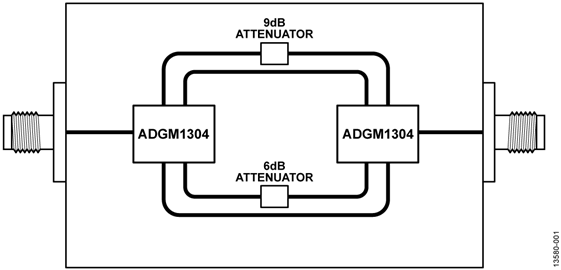
The circuit shown in Figure 1 uses RF MEMS switches to route an RF signal between two surface-mount RF attenuators and two straight through paths.
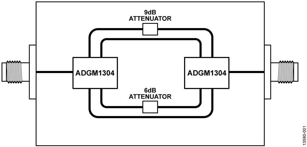
Attenuating RF signals is commonly done in RF test instrumentation and receiver front ends to protect downstream circuitry and to increase dynamic range. Using discrete attenuators and switches maximizes design flexibility and routing options. In the Figure 1 circuit, two ADGM1304 single-pole, four-throw (SP4T) RF MEMS switches in a back to back configuration yield four independently switchable paths between input and output. Two of the paths are straight through transmission lines, the third path contains a 6 dB attenuator, and the forth path contains a 9 dB attenuator. Key to realizing this application is the use of ultralow insertion loss and highly linear switches to multiplex between the different path options.
The switches must be as transparent as possible to the RF signal and add as little insertion loss and distortion as possible. The ADGM1304 switches offer best in class insertion loss of 0.26 dB typical at 2.5 GHz, and a third-order intercept (IP3) performance of 69 dBm typical. In addition to insertion loss and distortion, another key benefit that the MEMS switch brings to this application is its ability to operate down to true dc. This means the switches do not limit lower frequency operation in a typical RF instrumentation attenuator switching application, and enables the instrument to pass dc bias voltages when required.
The physical size of the ADGM1304 device at 4 mm × 5 mm × 0.95 mm yields a significant reduction in printed circuit board (PCB) area compared to traditional electromechanical relays switching solutions. In addition, the actuation speed of the ADGM1304 switch is 30 μs, a significant improvement over electromechanical relays, which are in the order of milliseconds and introduce significant time lag in measurement systems. The actuation lifetime of the ADGM1304 device is guaranteed for one billion cycles, which is a major improvement over electromechanical relays and significantly increases overall system reliability.
回路説明
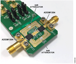
Figure 2 shows a close up photograph of the circuit evaluation board. The switches are marked in black. The ADGM1304 switches have a SP4T configuration; therefore, in a back to back arrangement, four individually selectable paths can be achieved. The surface-mount attenuators can be seen as the white components in Figure 2. They are manufactured by EMC Technology. The 6 dB and 9 dB attenuators (TS0606F and TS0609F, respectively) have an optimal performance frequency range of dc to 10 GHz and a peak power handling level of 2 W (33 dBm). The ADGM1304 MEMS switches have a 3 dB bandwidth of up to 14 GHz and a power handling level of 36 dBm (continuous wave) and are therefore ideally suited for
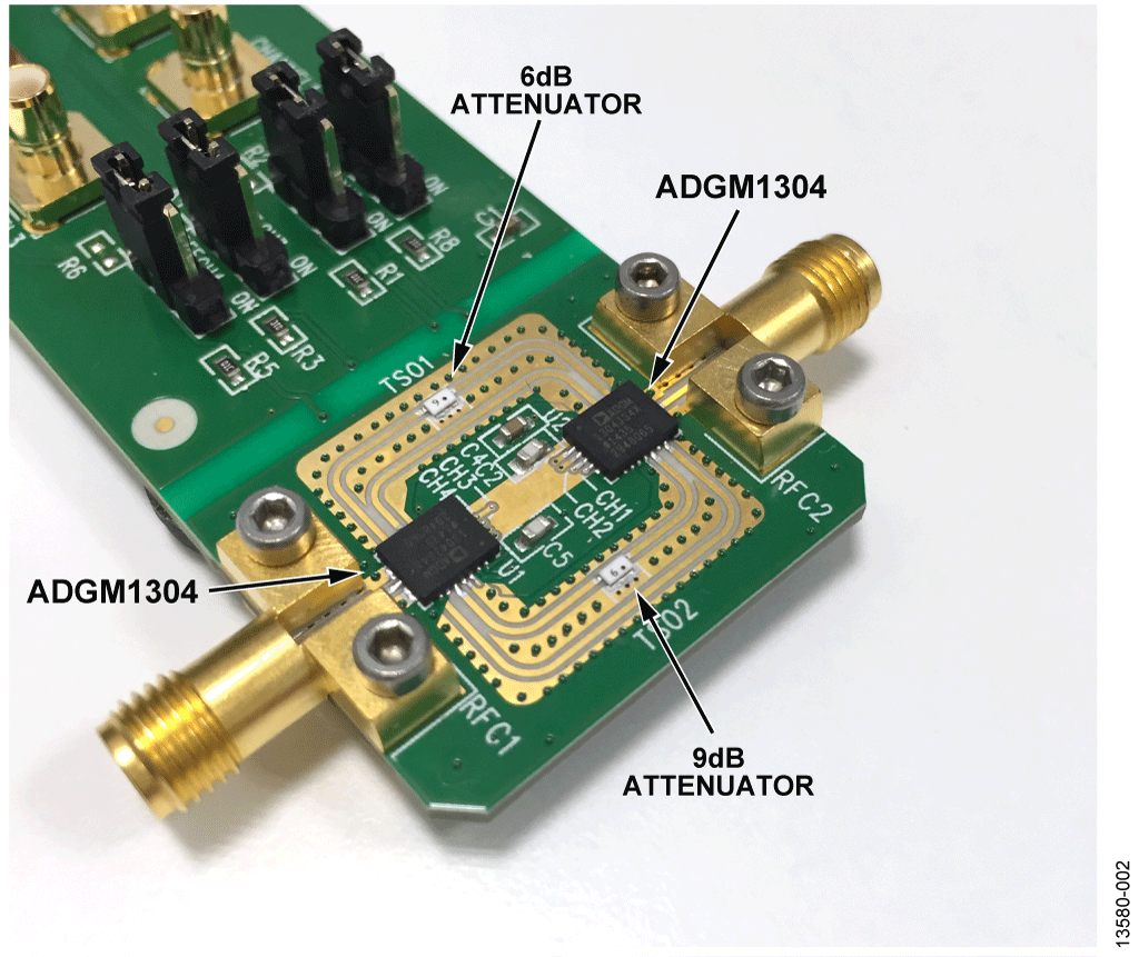
The RF edge launch SMA connectors are manufactured by Rosenberger (32K243-40ML5) and have a frequency range of dc to 18 GHz. The PCB material stack-up used is shown in Figure 3 and is the same as for the EVAL-ADGM1304EBZ evaluation board.
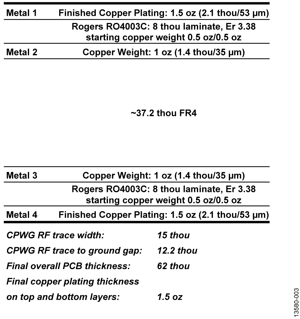
Figure 4 shows the full schematic for the PCB. The links marked CH1 to CH4 select between each of the four paths (two through paths and two attenuator paths). Because all these paths are independently controllable, they can all be on, all off, or any other combination thereof as necessary.
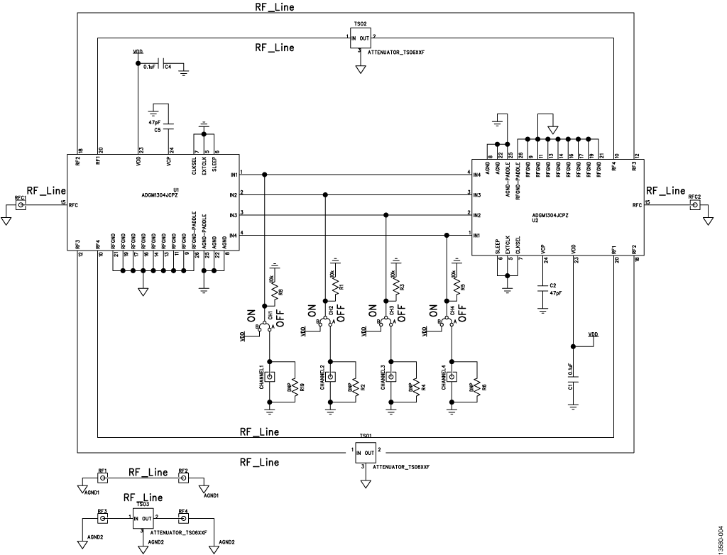
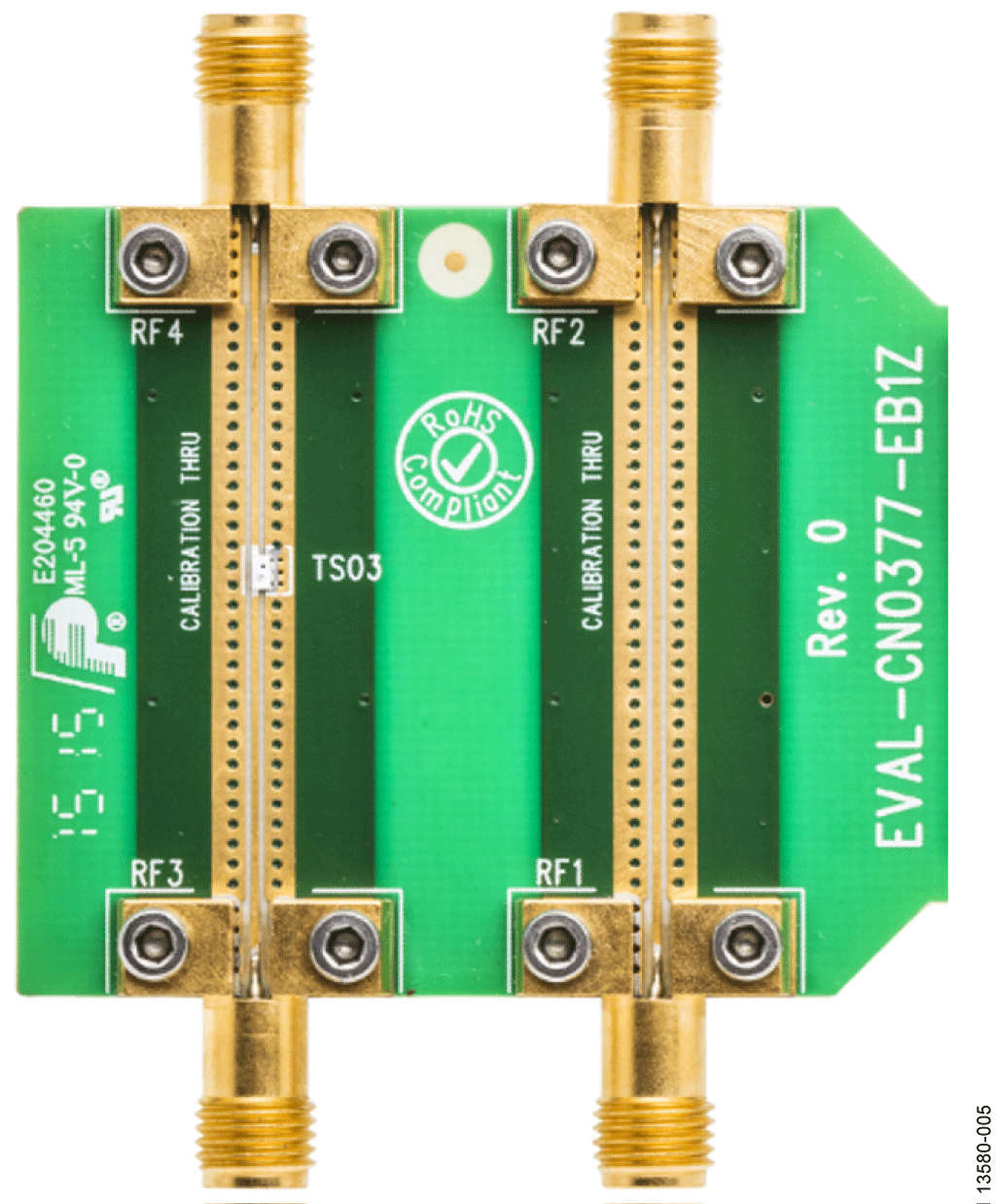
Also shown on the schematic in Figure 4 are the calibration structures. These consist of two transmission lines, each of which is the same length as the distance from input to output of the attenuator network. One of these transmission lines incorporates a 6 dB attenuator. The function of these lines is to compare the switchable attenuator performance to the ideal case where no switches are present. Figure 5 shows a photograph of these calibration transmission lines; the line on the left contains the 6 dB attenuator and can be seen as the white rectangle in the center of the line.
Test results with all combinations of paths, including comparison calibration line frequency performance, are shown in Figure 6.
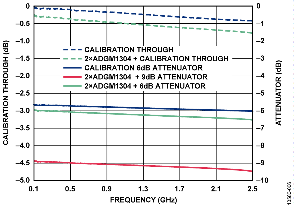
The dotted blue insertion loss trace at the top corresponds to the calibration through line, which is the ideal case with no switch present. The dotted green insertion loss trace is two ADGM1304 devices in a through line configuration. There is an approximate increase in insertion loss of only 0.3 dB at 2.5 GHz.
The solid blue line corresponds to the calibration line that contains the 6 dB attenuator. The corresponding switches plus attenuator network is the solid green trace. The insertion loss plots are referenced the right hand side dB axis. Again, the loss the two switches add is small and monotonic.
The 9 dB switching attenuator network is shown in red. As higher attenuator values are used the loss of the switches becomes less visible due to the fact of its small magnitude compared to the attenuator value.
The board is fully functional above 2.5 GHz, but because the switch is an unterminated reflective switch, the off channels can give rise to resonances in the insertion loss at higher frequencies.
バリエーション回路
Different values of attenuators can be used in this circuit. As a general rule the maximum attenuator value that can be used is limited by the off isolation of the back to back switches. Another variation of this circuit would be instead of switching between different RF attenuators, RF filters can be used. Filter bank switching is a common application and one where the ADGM1304 can also bring value because of its low insertion loss, operation to dc, high linearity performance, and small size.
回路の評価とテスト
The circuit board is designed to be connected to a vector network analyzer (VNA) via SMA compatible connectors. The SMA connectors on the board are female. To switch between each of the attenuators and through channels, there are four links marked CH1 to CH4 which can be manually changed to drive the parallel logic inputs of the switches. In addition, the switches can be controlled using digital signals input through the SMB connectors on the board.
Equipment Needed
- Vector network analyzer (VNA), Keysight 8753E with 85033D 3.5 mm calibration kit, or equivalent
- EVAL-CN0377-EB1Z evaluation board
- Power supply (3.3 V)
- Coaxial RF cables with 3.5 mm type connectors
Setup and Test
The test setup is shown in Figure 7. The VNA can only be connected to the circuit evaluation board through 3.5 mm connector compatible cables. Before starting to test the circuit evaluation board, a full two-port s-parameter error correction calibration of the VNA to the end of the cables is be required. Refer to the VNA manufacturer guidelines for how to perform this error correction calibration.
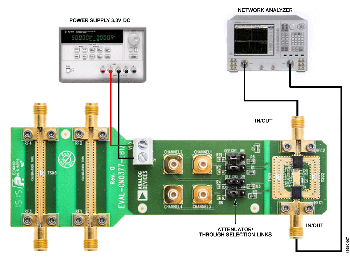
The circuit evaluation board is powered from a 3.3 V supply, and Table 1 shows the logic states for each link on the board to enable each of the attenuators and through paths.
| Attenuator/Through Path | Link |
|||
| CH1 | CH2 | CH3 | CH4 | |
| 6 dB (TS01) | 0 | 0 | 1 | 0 |
| 9 dB (TS02) | 1 | 0 | 0 | 0 |
| Through 1 (TS01) |
0 | 0 | 0 | 1 |
| Throught 2 (TS02) | 0 | 1 | 0 | 0 |


