Expanding TINI's IO Capability
要約
The TINI DS80C400 microcontroller evaluation (EV) kit (comprised of the TINIm400 module and TINIs400 socket) provides an excellent platform for evaluating the TINI hardware and software. The EV kit is, however, limited by scarce general-purpose IO (GPIO) pins. This application note explains how to add a CPLD (complex programmable logic device) to the socket board to provide a 32-bit, parallel IO interface.
Introduction
The DS80C400 evaluation kit combines the TINIm400 reference board and the TINIs400 socket to provide an excellent platform for the evaluation of the TINI runtime environment and the development of TINI-based applications on the DS80C400 networked microcontroller. One drawback to the TINIm400/TINIs400 pair is its limited number of general-purpose IO (GPIO) pins. The TINIs400 socket only contains a few pins that can easily be used as GPIO; most of the IO pins on the socket are spread across the board and intended for other functionality (for example, the I²C pins at J27 or the external interrupt pins at J4).
This application note demonstrates step-by-step how to use a complex programmable logic device(CPLD) to configure the hardware and develop the software needed to provide 32 additional GPIO pins to the TINIs400 socket board.
Hardware Setup
The first step in expanding TINI's IO capability is to populate four extra devices on the TINIs400 socket board: a CPLD, a power regulator, and two headers. The TINIs400 socket board includes pads and wiring for adding these devices which are not populated on the boards sold by Dallas Semiconductor. The devices are not populated because many applications either do not require expanded IO capability or use custom board designs.
Page 7 of the TINIs400 schematic¹ details the devices required for expanding TINI's IO capability. The schematic calls for a Xilinx® XC2C64 CoolRunner®-II CPLD in a 100-pin VQFP package. The TINI hardware has been tested with both the XC2C64 and the larger XC2C128, and should support any other size device with the same pinout and package.
There are three headers associated with the CPLD, two of which will need to be populated:
- J30 JTAG programming connector. The XC2C64 CPLD is programmed through a JTAG interface. The J30 connector provides pins for the JTAG signals TMS, TCK, TDI, and TDO. We will discuss this in greater detail in the section below entitled, Programming the CPLD.
- J28 expanded IO connector. This connector provides access to 32 pins on the XC2C64 device. We will program the CPLD to provide a read/write interface to these pins.
- J29 extra IO connector. This connector provides 16 additional connections to the XC2C64, which will not be used in this project.
Besides the J30 and J28 headers, there are additional devices that need to be populated:
- U2 MAX1792EUA18 regulator
- U12 Xilinx CPLD
- C40 to C57 capacitors. These capacitors, which are only required for using the CPLD, should already be placed on the TINIs400 socket board that you received from Dallas Semiconductor. If they were not properly placed or are missing, you might not have noticed during other TINI development.
CPLD Configuration
A CPLD is a programmable logic device. Think of it as programmable hardware with very flexible internal logic, which allows it to implement a wide range of functions with simple reprogramming. We can use a CPLD to implement 32 flip-flops to store logic levels that will be driven on the CPLD's output pins. We use Verilog, a hardware description language (HDL), to describe the function that the CPLD will implement. Tools from Xilinx will convert the Verilog source code into a binary form used to configure the CPLD.
On the TINIs400, the XC2C64 is connected to the memory bus of the TINI microcontroller, the DS80C400. This connection allows TINI programs to access the CPLD by writing and reading at specific addresses. Therefore, the CPLD must be programmed to respond when the address lines select it; the CPLD must latch the data bus signals written to it, and it must drive the port inputs onto the bus when it is read.

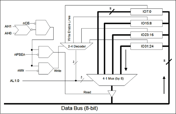
Figure 1 shows the block diagram for the function which the CPLD needs to implement. The blocks in the upper right (IO7:0, IO15:8, IO23:16, IO31:24) represent flip-flops that will store values to be driven to the output. Each of these 8-bit register banks is connected to the data bus. When enabled by the proper address lines and the write strobe (nWr), the contents of the data bus are latched into the registers. The input levels of the IO pins are sensed and fed to a 4:1 multiplexer, where the low bits of the address select the 8-bit value to pass to the data bus. If the CPU is requesting a read (qualified by the address lines and the nPSEN signal), the multiplexer's output is enabled and drives the data bus.
Although 10 address lines (not including the chip enables) are connected to the CPLD, this demo application will only use four of those lines. A17:A16 are the upper address lines used along with chip enable 6. When address bits A17:A16 are low and nCE6 is active (low), the CPLD is selected, although the CPLD takes no action unless the read or write signals are active as well. The other two address bits, A1:A0, select one of the four 8-bit registers as a target for writes or a source for reads. This address scheme means that many addresses will activate access to the four 8-bit registers. Table 1 summarizes this address flexibility.
| Register | A21 | A20 | A19 | A18 | A17 | A16 | A15 | A14 | A13 | A12 | A11 | A10 | A9 | A8 | A7 | A6 | A5 | A4 | A3 | A2 | A1 | A0 |
| IO7:0 | X | X | X | X | 0 | 0 | X | X | X | X | X | X | X | X | X | X | X | X | X | X | 0 | 0 |
| IO15:8 | X | X | X | X | 0 | 0 | X | X | X | X | X | X | X | X | X | X | X | X | X | X | 0 | 1 |
| IO23:16 | X | X | X | X | 0 | 0 | X | X | X | X | X | X | X | X | X | X | X | X | X | X | 1 | 0 |
| IO31:24 | X | X | X | X | 0 | 0 | X | X | X | X | X | X | X | X | X | X | X | X | X | X | 1 | 1 |
Since TINI libraries and operating firmware configure the DS80C400 for 2MB per chip enable, and since the DS80C400's address range is 24-bits (16 MB), the eight chip enables represent the upper 3 bits of the address. To activate chip enable 6, the high 3 bits of the 24-bit address must be 110b.
Although Table 1 indicates that multiple addresses will activate the registers, we only use the following addresses for the registers:
- Address C00000h → IO7:0
- Address C00001h → IO15:8
- Address C00002h → IO23:16
- Address C00003h → IO31:24
Verilog Coding
There are six Verilog files used to implement the 32-bit GPIO function in the CPLD. The files are included in the source code for this application note, and are accompanied by project files for Xilinx WebPACK® (see discussion below). The Verilog source files in this project are:
- Buffer8.v: 8-bit buffer used to connect the data bus from TINI to the four 8-bit registers
- Mux2x8.v: 2-to-1 multiplexer used to select between two 8-bit busses
- OneO4e.v: 2-to-4 decoder, which outputs one active signal depending on the low address bits
- Reg8OD.v: 8-bit pseudo-open-drain flip-flop array used to store output values
- TSBuffer8.v: 8-bit tri-state buffer used to drive input values onto the data bus
- CPLD.v: top-level connect between the blocks
The most interesting Verilog source file is CPLD.v. It contains definitions for inputs, outputs, and nodes, and it instantiates the blocks defined in the other files. This source file is also where the write and read pulses are extracted:
    assign Reset  = ~nRstOut;        // make a hi-active Reset
    assign IOBank = ~nCE6 & ~|AH;    // decode the I/O bank
    assign ReadT  = IOBank & ~nPSEn; // qualify Read strobe
    assign WriteT = IOBank & ~nWr;   // qualify Write strobe
The signal ReadT is then used as the enable to the tri-state buffer, driving the sensed input values onto the DS80C400's data bus:
    // Tri-State data bus to TINI needs this buffer
    TSBuffer8 U4(ReadT, DataToTINI, D);
The signal WriteT is fed to the four 8-bit register banks as the clock signal.
    // 4 8-bit pseudo-open-drain output drivers
    Reg8Out    U6(Reset, ~WriteT, Enable[0], DataFromTINI, UIO[ 7: 0]);
    Reg8Out    U7(Reset, ~WriteT, Enable[1], DataFromTINI, UIO[15: 8]);
    Reg8Out    U8(Reset, ~WriteT, Enable[2], DataFromTINI, UIO[23:16]);
    Reg8Out    U9(Reset, ~WriteT, Enable[3], DataFromTINI, UIO[31:24]);
One other important source file (though it is not a Verilog file) is CPLD.ucf. This file maps between the signal names declared in CPLD.v and the actual pins of the XC2C64 device. Here are the definitions for the address lines and a few of the IO pins:
    NET "AL<1>" LOC = "P30";
    NET "AL<0>" LOC = "P32";
    NET "AH<1>" LOC = "P37";
    NET "AH<0>" LOC = "P39";
    NET "UIO<5>" LOC = "P43";
    NET "UIO<6>" LOC = "P49";
    NET "UIO<7>" LOC = "P50";
    NET "UIO<8>" LOC = "P52";
    NET "UIO<9>" LOC = "P53";
Note that these pin definitions come directly from page 7 of the TINIs400 schematic. For instance, the schematic shows that address lines 3 through 0 (A[3:0]) are connected to pins 28, 29, 30, and 32. The listing above shows that we define the signals for the two lowest address lines (AL<1> and AL<0>), which are mapped to pins 30 and 32 on the CPLD.
Programming the CPLD
Project files for the CPLD programming are provided in the CPLD directory of the source code for this application note . You can use Xilinx's free WebPACK tools to build and program the CPLD. This application note was developed with version 6.3.03i. Later versions of Xilinx tools should be suitable as long as they support the CoolRunner 2 CPLD family.
Hardware Connection
We used an Avnet Avenue JTAG programming cable to connect our computer's parallel port to the JTAG pins of the CPLD. A JTAG programming cable comes with many CPLD or FPGA evaluation kits. Our programming cable is shown in Figure 2.


Figure 3 shows the connection required between the programming cable and the TINIs400 socket board. Signals are labeled so any other programming cable can be used. The TINIs400 socket board expects VCC to be 3.3V.


Loading the Project
To load the project, go to the File menu and select Open Project. Browse to the source files for this application note and select parallel32.npl. The project is now open and ready to build. The rest of this section describes how to configure a brand new project. You can skip this presentation and go directly to the following section to learn how to program the CPLD.
The following instructions will create a new project, based on the source code provided with the application note.
- Under the File menu, select New Project.
- Select the directory where you want to build the new project, and enter a project name. A new directory will be created with the name of the project. Make sure that the Top Level Module Type is HDL. Click Next to continue.
- This menu lets you select the device and package that your project will be targeting. For the Device Family, select CoolRunner 2 CPLDs. Next select your Device from the list provided—probably the XC2C64, XC2C128, or equivalent device. For the Package, select VQ100, which is the package assumed for the TINIs400 socket. See Figure 4 for the rest of the configuration options used in this application note. Once complete, press Next to continue.
- The next window asks for any new files to be created in the project. Since all the source files are provided, click Next without adding any new files.
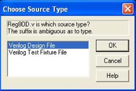
- The following window asks you to add any existing source files. Click the Add Source button and add all of the Verilog files (as listed in the Verilog Coding section above) and the CPLD.ucf file from the source distribution. Once added, the program may ask, File.v is which source type? The suffix is ambiguous as to type. Select Verilog Design File and click OK (see Figure 5). Once it has classified all the input files, click Next to continue.
- The next window summarizes the new project. Review the information and click Finish.
- As long as the UCF file was added in Step 5 above, the program will ask you to associate it with the source it affects. Select CPLD from the list and click OK.


At this point, the project has been created and configured. You can now edit, build, and synthesize your design.
Device Programming
Follow the instructions in this section to synthesize the CPLD project and program the XC2C64 device. Make sure that the programming cable is connected as described in the earlier section, Hardware Setup.
To program the CPLD:
- In the Project View (typically the top left window), select the Module View tab. Under the Module View, select the main file, CPLD.v.
- In the Process View window (typically below the Project View window), expand the Implement Design branch and double click on Generate Programming File. This will run all the processes required to convert the Verilog source code to a binary file that will program the CPLD. As the processes run, marks will appear to the left of the process to describe the results of their execution. A green check mark means that the process terminated successfully without errors or warnings. Yellow exclamation points mean that the process terminated successfully, but with warnings. A red X means that the process did not terminate successfully due to errors.
- Once the processes terminate and the programming file is successfully generated, double click Configure Device (IMPACT).
- A window will appear which reads Configure Devices. Select the option Boundary Scan Mode and click Next.
- From the next window (Boundary-Scan Mode Selection) select Automatically connect to cable and identify Boundary Scan chain, and click Finish.
- If the device is properly connected, iMPACT will show a popup box that reads, "There was one device detected in the boundary-scan chain. iMPACT will now direct you to associate a programming or BSDL file with this device...." Click OK.
- A File Dialog Window should open to your current project directory (if it does not open to this directory, browse to the correct location). Select CPLD.jed from the window by double clicking on it.
- Right click on the Xilinx chip picture and select Program.
- Make sure that Erase Before Programming and Verify are checked, and that no other boxes are checked. Click OK.
- A programming status bar will appear, and after a few seconds (less than 20) the programming will be complete and the CPLD will be configured.
When you move on to your own CPLD functional designs, make sure that the CPLD code releases the address, control, and data signals to a high impedance state when the DS80C400 is not talking to the CPLD. Failing to do this is a common error resulting in frustrating symptoms, such as the board being held in reset or rebooting randomly. When this problem occurs, simply erase the CPLD to stop the symptoms.
Debug Board
A simple bank of 32 LED's demonstrates TINI's expanded IO capability. The demo board uses four LED banks and four resistor packs to indicate the state of each of the CPLD's IO pins. The LED board (attached to a TINIs400) is shown in Figure 6.


The schematic for this simple board is included in the source code for this application note. Note that the resistor values are suggested values; resistances too high will result in extremely dim displays, and resistances too small will drain too much current from the TINI power supply and stop its execution.
Software Interface
Having implemented this simple memory interface, the software to access our extended IO pins becomes quite simple, and will be implemented in assembly language (for integration into a Java application as native methods).
Table 2 shows the native Java methods defined for the interface.
| Function | Arguments | Returns | Description |
| program0 | int x | none | Write the input value x to the address C00000h (IO7:0). |
| program1 | int x | none | Write the input value x to the address C00001h (IO15:8). |
| program2 | int x | none | Write the input value x to the address C00002h (IO23:16). |
| program3 | int x | none | Write the input value x to the address C00003h (IO31:24). |
| Read0 | none | int | Reads from address C00000h. |
| Read1 | none | int | Reads from address C00001h. |
| Read2 | none | int | Reads from address C00002h. |
| Read3 | none | int | Reads from address C00003h. |
Note that the same job could also be accomplished with two functions: program(int address, int x) and read(int address). However, for this application we chose to assign one function per address, which allows applications to abstract the different addresses as functional registers.
The assembly code for each program and read function is quite simple. The code only requires the data pointer to be loaded with the correct address, and then a movx instruction activates the memory bus.
    Native_program0:
      clr    a                       ; request first parameter
      lcall  NatLib_LoadPrimitive    ; load parameter into r3:r0
      mov    dptr, #0C00000h         ; point to memory mapped peripheral
      mov    a, r0                   ; move low byte of source into accumulator
      movx   @dptr, a                ; write to memory mapped peripheral
      clr    a                       ; indicate no error condition
      ret                            ;

      ...

    Native_read0:
      mov    dptr, #0C00000h         ; point to memory mapped peripheral
      movx   a, @dptr                ; read from memory mapped peripheral
      mov    r0, a                   ; move into low byte of result
      clr    a                       ; indicate no error condition
      mov    r1, a                   ; unsigned extend to 32-bits
      mov    r2, a                   ; unsigned extend to 32-bits
      mov    r3, a                   ; unsigned extend to 32-bits
      ret                            ;
Example Application
The example application is in the folder javacode in the source code. This application writes incrementing values to the four LED banks. The values update every 500 milliseconds, so it should be easy to know if the application is running correctly.
Since this application includes both native methods and Java code, the build process is somewhat more complex than Java-only programs. A build batch file is included with the source code, but will require some modification for your development system, as detailed below:
-
c:\work\tini\tini1.16
    ative\bin\win32\macro -Ic:\work\tini\tini1.16
    ative\lib\ cpld.a51
Change the directories to point to the location of the macro preprocessor and the native library include files stored on your hard drive. These items are part of the standard TINI SDK available at ftp.dalsemi.com/pub/tini/index.html. -
c:\work\tini\tini1.16
    ative\bin\win32\a390 -f 1.16 -p 400 -l cpld.mpp
Change the directory to point to the location of the a390 assembler program. This is stored in the same directory as the macro preprocessor. -
del *.class
Removes previously existing classes from the current directory. -
javac -bootclasspath C:\work\tini\tini1.16\bin\tiniclasses.jar demo.java
Builds the source file demo.java against the TINI class files. Change the directory to point to the API classes for TINI, which is part of the TINI SDK. -
java -classpath C:\work\tini\tini1.16\bin\tini.jar;%classpath% TINIConvertor -n cpld.tlib
Builds the TINI executable combined with the native library for interfacing with the CPLD. The Java code only needs to call the function
-f . -o demo.tini -d C:\work\tini\tini1.16\bin\tini.dbSystem.loadLibrary("cpld.tlib")to access the CPLD's expanded IO pins. Again, the directories need to be changed to point to the tini.jar tools file and the tini.db class database that come with the TINI SDK.
Conclusion
The combination of a TINI and a CPLD provides a simple interface to expanded and highly flexible IO capabilities. Expanded IO is not, however, the limit of possibilities when using a programmable logic device. CPLDs can be used for many logic functions and state machines. Combined with TINI's network stack, a Java virtual machine, and operating system, a CPLD allows TINI systems to be highly configurable and flexible.
著者
