AN-2595: ADRV904x Power Application Note
Scope
This application note is a document that assists in the design of the ADRV904x power supplies and discusses the method to determine the total current requirements and the stability of the power supply. This application note also explains the recommended power-supply configuration for three modes of transceiver operation: time division duplex (TDD), frequency division duplex (FDD), and mixed mode.
Other power-supply topics are covered in the ADRV904x system development user guide in the following sections:
- Power supply domain connections − Provides pin numbers and names and a brief description.
- Power supply sequence − Describes the sequence in which supplies are applied to transceiver.
- Power supply architecture − Provides a diagram of all power supply connections.
- RBIAS setup − External components for controller internal reference.
- Power management layout design − Discusses the evaluation board (EVB) layout considerations.
Power Introduction
The ADRV904x evaluation board provides a reference design for power-supply design. Since this evaluation system must accommodate a broad customer set of use cases, the evaluation board is required to customize for a particular application.
Power-supply requirements for the ADRV904x can be divided into three following requirements categories:
- Maximum power for each domain
- ± Tolerance of the supply voltage
- Ripple of the supplies
Each of these categories is covered in separate sections in this application note.
Due to added digital front end (DFE) plus processor features, VDIG_0P8 current can be as high as 19 A. Extra VDIG_0P8 pins are added in ADRV904x and two reservoir 100 µF capacitors are added for decoupling. Because of the high-current drain, the VDIG_SENS_0P8 pin is added to compensate trace I×R drop that can occur in the 0.8 V supply due to supply routing.
The ADRV904x uses the analysis control evaluation (ACE) software developed by Analog Devices, Inc., extended by the ADRV904x specific board plugin. This software evaluation tool is referred as the configurator in this document. The user must install ACE and become familiar how to use it. The instructions to get and install the software can be found on the ADRV904x product page.
Maximum Power Requirements
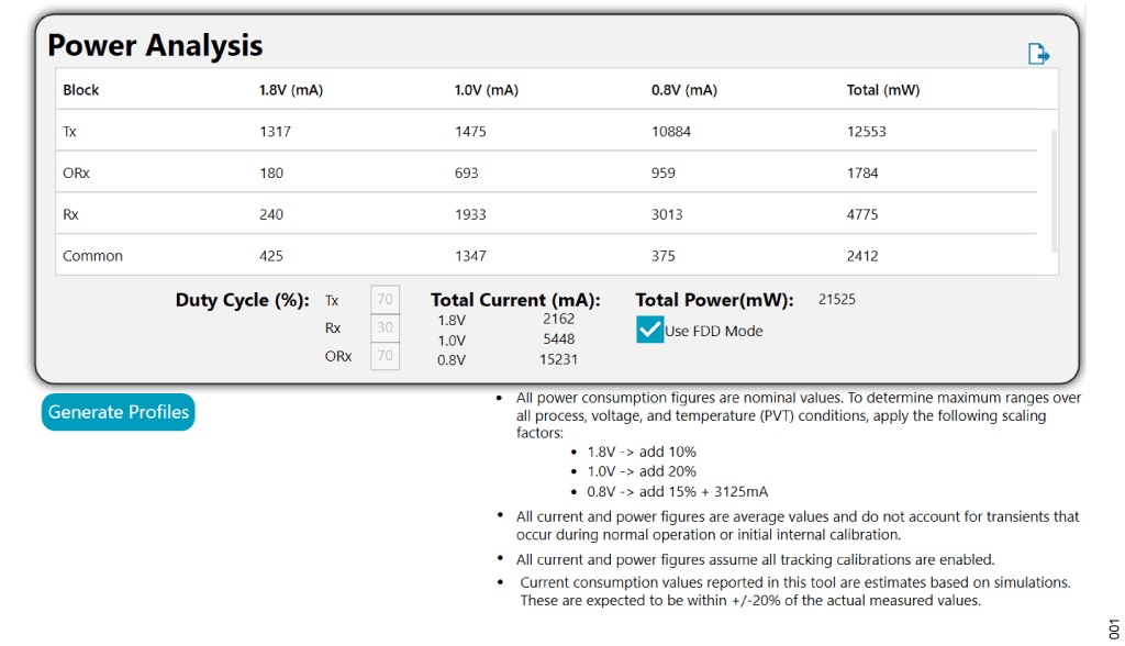
The configurator is used to load a previously generated use case. Subsequent configurator pages can be used to customize by configuring the local oscillator (LO), carrier digital upconverter (DUC), transmitter bandwidth, and JESD settings, to arrive at and validate a required ADRV904x use case. Current is dependent on the configuration, therefore a power analysis page is provided to give current drain per use case. Figure 1 shows the configurator power analysis tool. Here each domain current is listed for each of the signal chain blocks and total current is provided in Figure 1. A checkbox is provided to select FDD mode. This enables all signal blocks, therefore providing the highest current drain for the use case. Alternatively, the TDD duty cycles for the transmitter, receiver, and observation path receiver can be adjusted from 0% to 100% providing an average current for a TDD frame. Setting duty cycles to 100% gives similar results as checking FDD mode. The numbers provided in the table are typical numbers. To determine maximum values to account for IC manufacturing process, voltage variation, and temperature variation (PVT), an additional factor must be added. These values are shown in Figure 1, for 1.8 V add +10%, for 1.0 V add 20%, and for 0.8 V add 15% plus an additional 3125 mA for what is referred to as digital leakage current.

Power-supply Output Tolerance
Power-supply tolerance refers to the minimum and maximum range the voltage of each supply can drift. These specifications are listed in the ADRV904x data sheet under the power-supply specifications section. Internal circuits of the transceiver are power cycled during initialization. The supply design must maintain the specification ranges during these current transitions. It is recommended to observe each domain during initialization with an oscilloscope as close as possible to the IC for power-supply compliance. Analysis has shown that voltage that exceeds the 1.0 V supply input (collectively referred as VDDA_1P0) can degrade the lifetime of the device if it persists indefinitely. A peak voltage maximum duty cycle must be maintained to avoid reducing the lifetime of ADRV904x. The table under absolute maximum ratings section in the ADRV904x data sheet, it shows the maximum duty cycle of the 1.0 V supply to maintain a 10-year lifetime, where the percentage is the amount of time the supply voltage exceeds the rated maximum. The 0.8 V and 1.8 V maximum value is listed in the absolute maximum ratings table in the ADRV904x data sheet.
Power-supply Ripple and Transient Settling
Integrated transceivers that generate their own local oscillators and clocks rely on stable power supplies. Signals on the supplies (that is, switching frequency harmonics) can modulate the phase of the LO or clock, creating local spurs on transmitter and receiver signals (most critical for global system for mobile (MC-GSM) systems). These characteristics are not dependent on transceiver architecture. They affect any system using LOs or sample clocks.
The following power supply characteristics can impact the transceiver clock and LO:
- Spurious Signals: Signals on the supplies (switching frequency harmonics) can modulate the phase of the LO or clock, creating spurs or broad-spectrum noise on transmitter and receiver signals.
- Settling Time: If supply voltage has not settled after a load step
(as described in TDD operation), the LO phase is not settled at
the transmitter and receiver mixers, which impacts beamforming
accuracy, transmitter and receiver error vector magnitude (EVM).
Variation in power-supply levels during operation can result in varying LO and clock delays. LO delay changes inversely with voltage level. Increased voltage results in less delay, whereas decreased voltage produces more delay. Clock and LO variations directly affect the phase variation on transmit and receive signals. Power-supply variation effects on relative and absolute phase are small compared to their impact on transmitter and receiver EVM. Therefore, phase variations are ignored for determining power-supply requirements and the focus is on EVM.
The 1.0 V and 1.8 V supplies are divided into two types: dynamic supply inputs connected to blocks that experience load steps during TDD operation, and static supply inputs that remain stable during TDD switching. Static inputs require the line regulation to be very good when TDD switching occurs to maintain performance. EVM can degrade if line voltage is varying during normal operation.
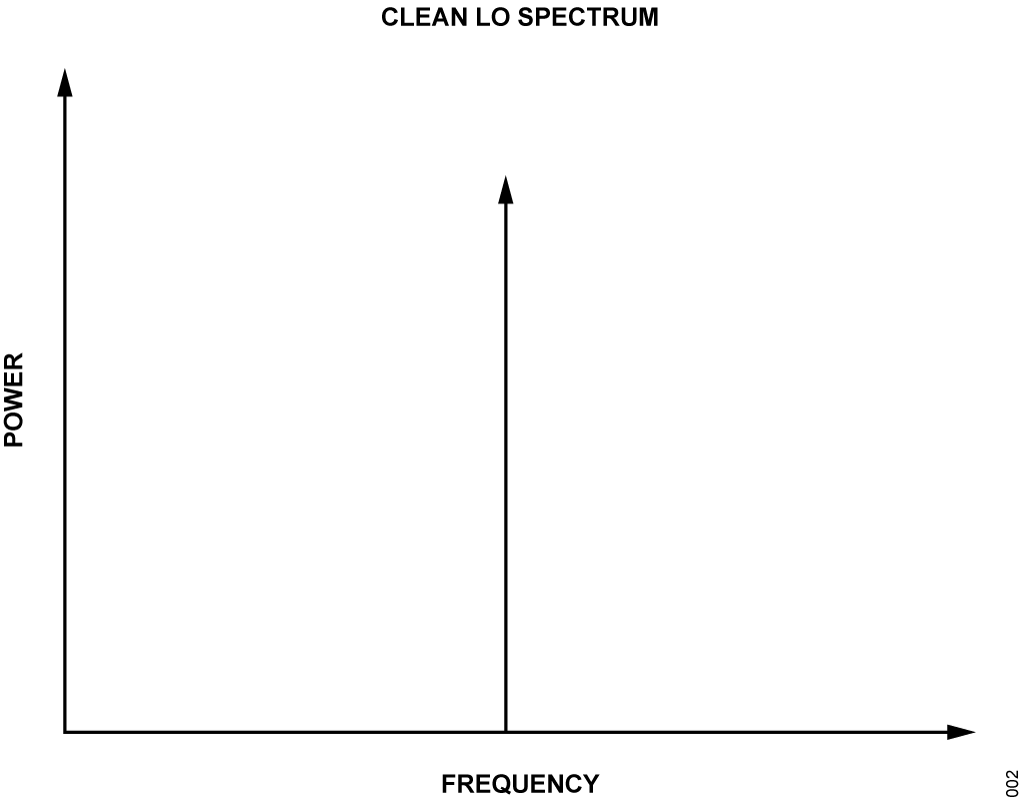
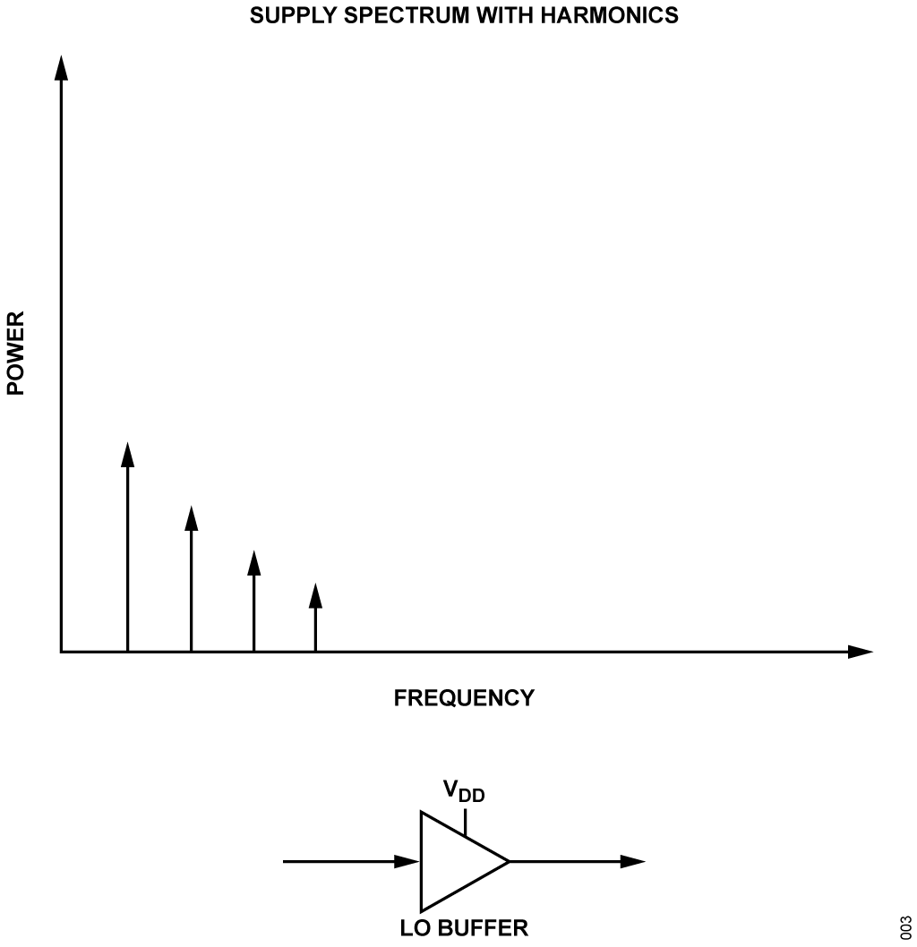
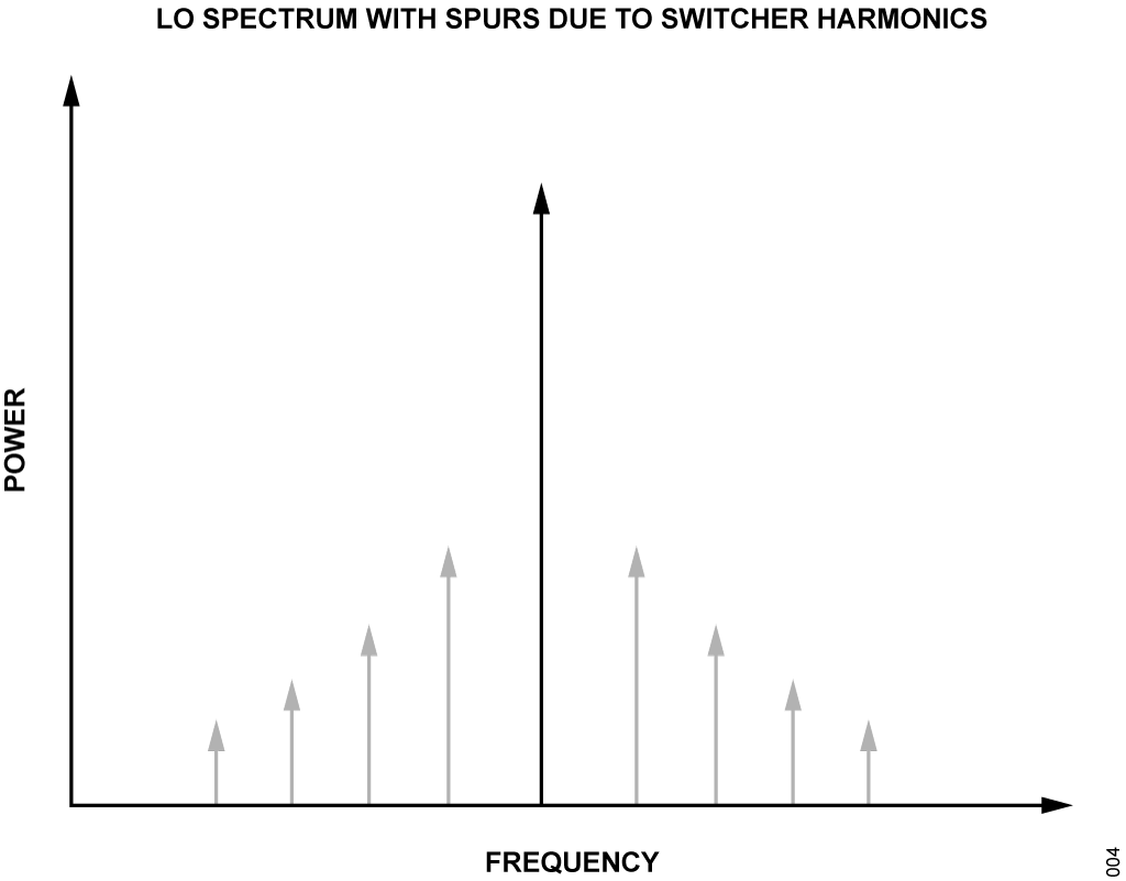
Figure 2 shows in the frequency domain a pure sine-wave tone. Figure 3 shows a possible frequency domain of a power supply that contains a specific ripple frequency and its harmonics. For the LO path, there is a case where AM to PM conversion can take place, which causes the power-supply ripple to be transferred to the LO as phase modulation. This is shown in Figure 4.


Spurious Signals
Table 1 provides the 1.0 V supply ripple to LO spurious sensitivity information. As LO frequency increases, the sensitivity becomes higher. The first column is the LO frequency, and the second column is the maximum spur level requirement options −70 dBc, −75 dBc, or −90 dBc. The next column is the typical µV RMS ripple that causes the spurious level. For example, for an LO frequency of 2.0 GHz a 100 µV RMS ripple on the 1.0 V supply causes a −75 dBc spur on the transmitter internal LO.
| Maximum Level of Each Supply Harmonic (µV RMS) | ||||
|---|---|---|---|---|
| LO Frequency (GHz) | Max LO Spur Level (dBc) | Tx – Internal LO | Rx – Internal LO | External LO – Rx or Tx |
| 1.0 | -70 -75 -90 |
356 200 36 |
445 250 44 |
285 160 28 |
| 2.0 | -70 -75 -90 |
178 100 18 |
222 125 22 |
142 80 14 |
| 2.7 | -70 -75 -90 |
132 74 13 |
165 93 16 |
105 59 11 |
| 3.5 | -70 -75 -90 |
102 57 10 |
127 71 13 |
81 46 8 |
| 4.9 | -70 -75 -90 |
73 41 7 |
91 51 9 |
58 33 6 |
| 6.0 | -70 -75 -90 |
59 33 6 |
74 42 7 |
47 27 5 |
Settling Time
It is much easier to show power-supply ripple using single frequency tones. But similar distortion can occur with a broadband spectrum that looks more like noise than discrete spurious tones.
Figure 5 is a diagram that shows the requirements of settling time of the 1.0 V supply domain. The disturbance is caused by turning on all the transmitter channels simultaneously during a TDD slot. A sudden drop in the 1.0 V supply occurs, when these circuits are enabled. First symbol transmitter EVM can be impacted by power-supply settling with large amplitude variation and long duration. Minimizing settling time and ripple are important for optimizing EVM.

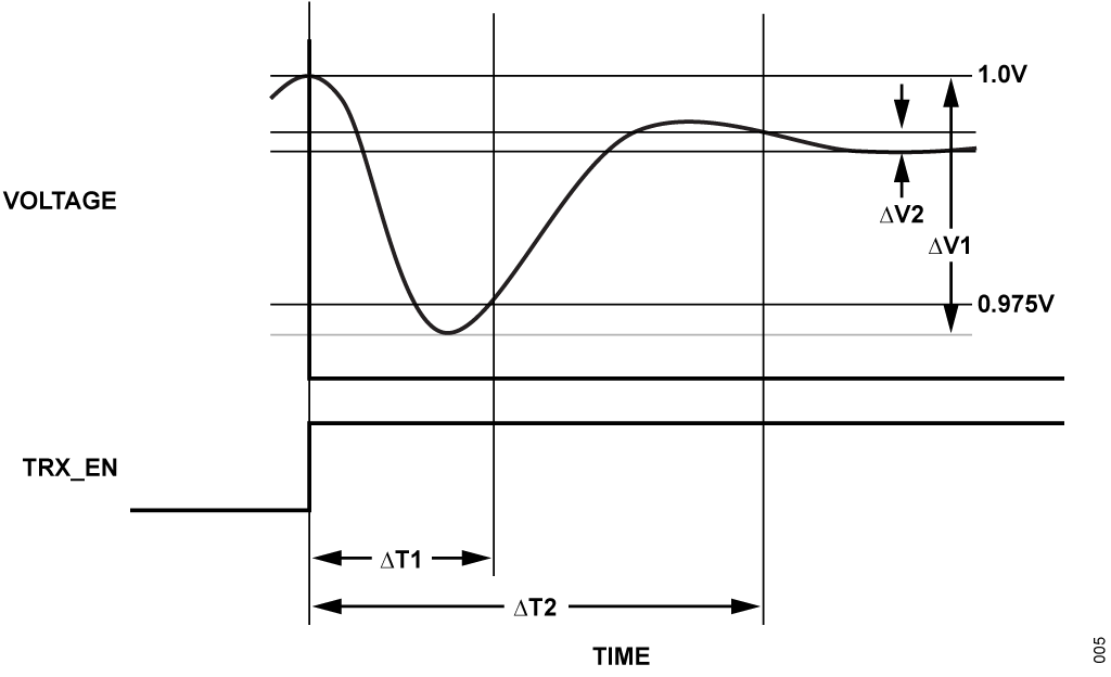
| Symbol | Description |
|---|---|
| ΔV1 | 1.0 V supply can exceed its ±2.5% tolerance but must return to within 2.5% before channel data operation is required. |
| ΔT1 | The settling time of 1.0 V supply to re-enter the supply tolerance range. |
| ΔV2 | The variation from the final settled supply value. It influences EVM of the first symbol, larger variation results in higher EVM. |
| ΔT2 | The power-supply settling time to fall within the ΔV2 range to meet first symbol EVM requirements. Value depends on system constraints. |
Transceiver channels typically target settling to within 2 µs. ΔT1 must be completed before this period for stable operation for both static and dynamic supplies. 1.8 V supply has similar behavior and requirements. Note that settling times account for both the regulator and transceiver settling but is measured at the device under test (DUT) input.
Table 3 shows the required settling for static supplies to achieve a 1% and 2% first symbol EVM target. Almost all the budget can be allocated to supply settling if the PLL integrated phase noise is significantly less than 1% (assume that this requirement is met). Settling is more critical for supplies listed under the static domain. Note that these targets are more difficult to achieve in TDD mode due to supply noise caused by load steps.
| LO Frequency (MHz) | 1% EVM: ΔV2 Limit (mV) Static Supplies | 2% EVM: ΔV2 Limit (mV) Static Supplies | ||
|---|---|---|---|---|
| N/A1 | 1.0 V | 1.8 V | 1.0 V | 1.8 V |
| 1800 | 4.4 | 15.2 | 8.8 | 30.4 |
| 2600 | 3.1 | 10.5 | 6.1 | 21.0 |
| 3800 | 2.1 | 7.2 | 4.2 | 14.4 |
| 4800 | 1.7 | 5.7 | 3.3 | 11.4 |
| 6000 | 1.3 | 4.6 | 2.7 | 9.1 |
| 1 N/A = not applicable | ||||
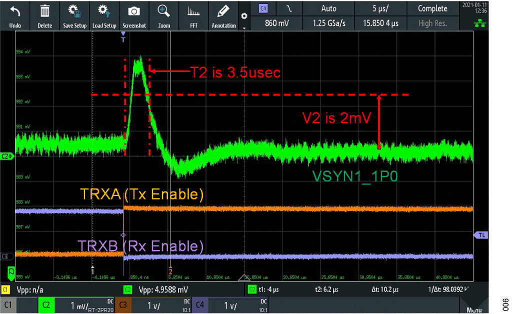
Figure 6 is an actual measurement of the 1.0 V supply pin to show a TDD transient response. The orange trace shows an OFF to ON transition of the transmitter enable pin. The green trace shows a release of the supply caused by a drop in current. The blue trace is the receiver enable going from ON to OFF. It takes approximately 3.5 µs for the supply to setting to within 2 mV of the final value. With a 3800 MHz LO, a user can expect to see 1% EVM degradation caused from this supply settling.

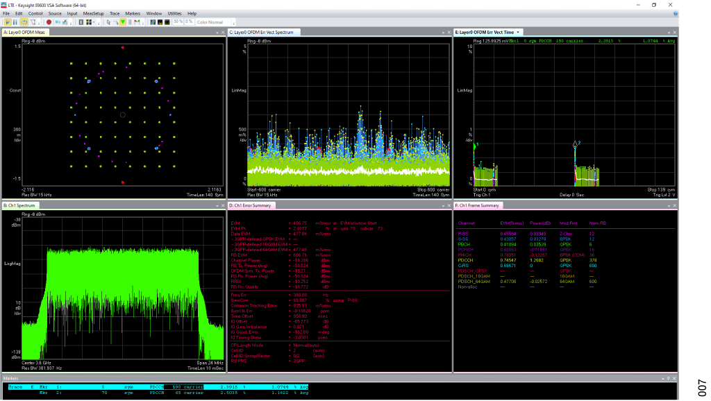
The upper right EVM vs. symbol plot of Figure 7 shows that a glitch in the TDD EVM caused by the supply transition. LTE is used for this measurement, which has a symbol time of 66.67 µs long. Therefore, this plot cannot show EVM with 1 µs resolution. All that can be seen is a peak and average of EVM for the first symbol. The peak EVM for the first symbol is 2.4% but the average EVM is approximately 1% (white trace). This agrees well with what a user expected from the supply measurements shown in Figure 5.

Power-supply Configuration
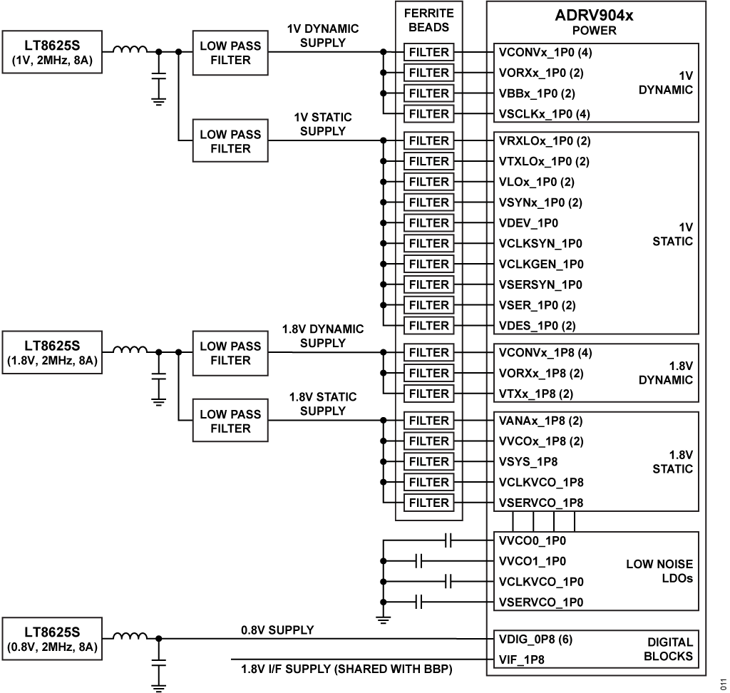
There are two main aspects of the power-supply design, hardware choice and printed circuit board (PCB) layout. The ADRV904x customer evaluation board is used as a reference for the information provided in this section. Any figures that have capacitor or resistor numbers are referring to the ADRV904x evaluation board schematics. The three power domains that are required are 0.8 V, 1.0 V and 1.8 V. These are all derived from the LT8627SP step-down silent switchers. These devices offer low noise and ultra fast transient response.
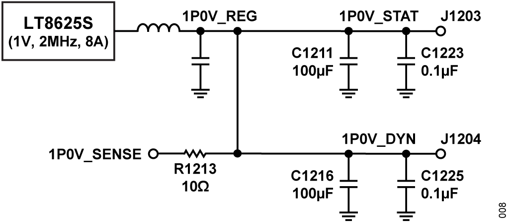
For the 0.8 V domain, two LT8627SP silent switchers placed in parallel provide over 30 A drive capability. The first regulator CLKOUT signal connects to second regulator sync/mode input, to line up both frequency and phase of the entire system. The two converters switch out of phase to reduce noise. The first LT8627SP PHMODE connected to ground for 180° phase shift clock output to the second device. Remote sense must be connected directly to VDIG_SENS_0P8.
For the 1.0 V and 1.8 V each use an LT8627SP. Power on/off sequence specified in the user guide is accomplished by 0.8 V regulator turns on by power_supply_enable from FMC, 0P8V_GOOD enables 1.0 V regulator, 1P0V_GOOD enables 1.8 V regulator, and 1P8V_GOOD lights an LED. Power down disables all regulators simultaneously.
The outputs of each of the regulators are then distributed to the balls of the ADRV904x through PCB traces and passive components. The passive components and connections can differ depending on the modes of operation of the ADRV904x.
TDD Mode
TDD is the case where all eight transmitter and receiver channels are operating in TDD mode. During TDD operation, some ADRV904x supply pins experience a current load-step from switching internal circuits on and off. These supply pins are referred to as dynamic. Supply pins that see no change in current during TDD operation are considered static. These two domains are described in the power management considerations section of the ADRV904x reference manual. First symbol transmitter EVM can be impacted by power-supply settling of large amplitude variation and long duration. Minimizing power-supply settling time and ripple are important for optimizing EVM. Additional filtering component is added to the original EVB to allow experiments to optimize power-supply design performance. Experiments are completed and resulted in a reducing the number of components on the EVB.
The following recommendations for EVB bill of materials (BOM) changes and the recommended configuration for TDD mode on the customer system board are developed from these experiments. The three major changes on the ADI evaluation board are:
- Eliminate static and dynamic low-pass filters. Only capacitors are needed to reduce spurious signals from supply transients.
- LTE/5G systems can combine static and dynamic inputs on a single supply if proper routing and decoupling techniques are used.
- Ferrites can be removed from all supply traces into the IC to avoid supply ringing from TDD current pulse.
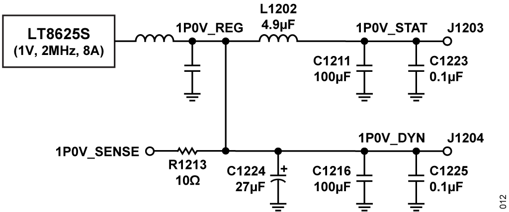
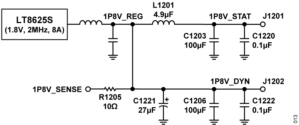
The details of the 1.0 V and 1.8 V connections are shown in Figure 8 and Figure 9 respectively. The filters have been simplified to only bypass capacitors close to the DUT as possible.


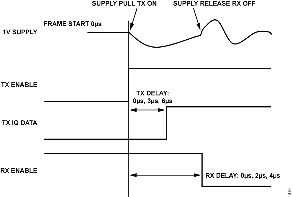
Transmitter EVM measurements are taken using 20 MHz LTE signal. Transmitter first symbol EVM measurements with the ADRV904x operating in pin mode TDD operation. Note that an LTE symbol is 66 µs in length, therefore, this is the finest time resolution that can be made for EVM vs. time. The diagram of the TDD timing used for the transmitter EVM measurement is shown in Figure 10. Time = 0 sec is defined to be the start of the TDD frame and all other delays reference this time position. Transmitter enable always occurs at the start of the TDD frame. Transmitter delay is the time in which actual IQ traffic is delayed from the start of the frame. This number is incremented from 0 µs, 3 µs, and 6 µs. Receiver delay is the time period from the start of the TDD frame to when receiver enable pins go low by that turning off the receiver channels. This delay is incremented from 0 µs, 2 µs, and 4 µs. A receiver delay of 0 µs results in the receiver channels being disabled as the same time as transmitter channels are enabled.

Average EVM for the entire time slot and average of the first symbol period are recorded in Table 4. The elevated first symbol EVM is due to power-supply settling. Longer transmitter delay (3 µs to 6 µs) allows power-supply transient to settle. Having transmitter enable and receiver disable times the same (receiver delay = 0 µs) result in best EVM performance. Rows 1 and 2 show the results with having ferrite beads installed. Rows 5 and 6 with ferrites removed. Rows 3 and 4 with ferrites removed on only three domains show some improvement in EVM. Green box highlights best performance are all ferrites shorted, receiver delay = 0 µs, transmitter IQ data delay of 3 µs to 6 µs. Having receiver delay > 0 µs results in longer settling and higher EVM since this causes a second disturbance to the supply rail when the receiver channels are turned OFF.
| Conditions EVB Ferrites Status | Measurement Transmitter IQ Data Delay | Rx Delay = 0 μs | Rx Delay = 2 μs | Rx Delay = 4 μs | ||||||
|---|---|---|---|---|---|---|---|---|---|---|
| 0 μs | 3 μs | 6 μs | 0 μs | 3 μs | 6 μs | 0 μs | 3 μs | 6 μs | ||
| All Ferrite Beads Installed | Average Slot LTE EVM% | 1.2 | 0.9 | 0.8 | 1.4 | 0.9 | 0.8 | 1.7 | 1.4 | 1.3 |
| Average First Symbol LTE EVM% | 5.5 | 3.2 | 1.9 | 6.5 | 3.6 | 2.8 | 8.5 | 7.2 | 5.9 | |
| VSYN0, VSYN1, VDEV Beads Shorted | Average Slot LTE EVM% | 1.3 | 0.8 | 0.7 | 1.2 | 0.8 | 0.7 | 1.4 | 1.0 | 0.8 |
| Average First Symbol LTE EVM% | 6.0 | 1.4 | 1.1 | 5.3 | 1.9 | 2.1 | 6.3 | 3.4 | 2.2 | |
| All Ferrite Beads Shorted | Average Slot LTE EVM% | 1.3 | 0.8 | 0.8 | 1.1 | 0.8 | 0.7 | 1.4 | 0.8 | 0.8 |
| Average First Symbol LTE EVM% | 5.7 | 0.87 | 0.68 | 4.8 | 1.3 | 0.64 | 6.6 | 2.7 | 1.5 | |
Using ADI silent switcher power-supply devices result in minimal transmitter delay due to their fast settling time.
FDD Mode
FDD is the case where all eight transmitter and receiver channels are operating in FDD mode. Transmitter EVM (RMS phase error) for MC-GSM system is not as critical as for LTE and 5G systems, however, there is a need to keep all power-supply coupled spurious content < −90 dBc. See Table 1 for an external LO a 14 mV RMS ripple causes a 90 dBc spurious. Passive low-pass filters are used to separate static and dynamic supplies and reduce interference due to varying loads on the dynamic supplies. FDD systems experience some dynamic domain noise due to ADRV904x internal calibrations or observation channels switching on and off. But load steps are not as large as in TDD mode, resulting in less variation. In addition, passive filters reduce spurious signals due to switcher harmonics of the regulators.
Figure 11 shows the design of the power supply for FDD mode of operation. A low-pass filter is inserted between the static and dynamic domains to isolate any transients from the dynamic domain from the static domain to keep any ripple below the specification. The details of the 1.0 V and 1.8 V isolation filter are shown in Figure 12 and Figure 13, respectively.


Multiband Mixed FDD and TDD Mode (Hybrid Mode)
Multiband mixed FDD and TDD is the case where there are a combination of channels on one IC running in TDD and FDD mode. The concern is that the transitions in TDD mode degrade the FDD static supplies and result in degraded phase error and spurious when using the suggested TDD or FDD mode power-supply configuration.
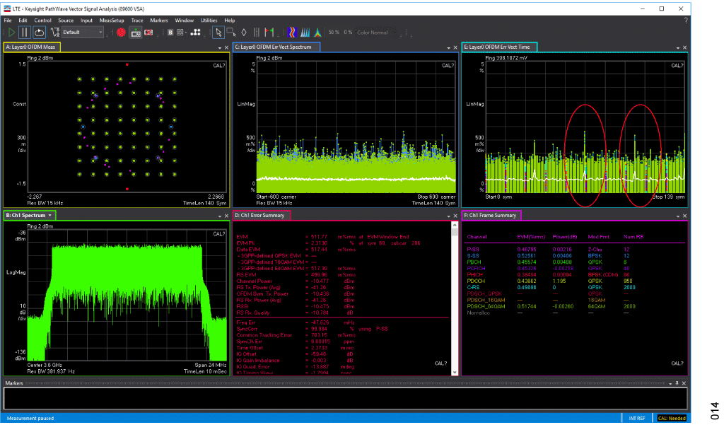
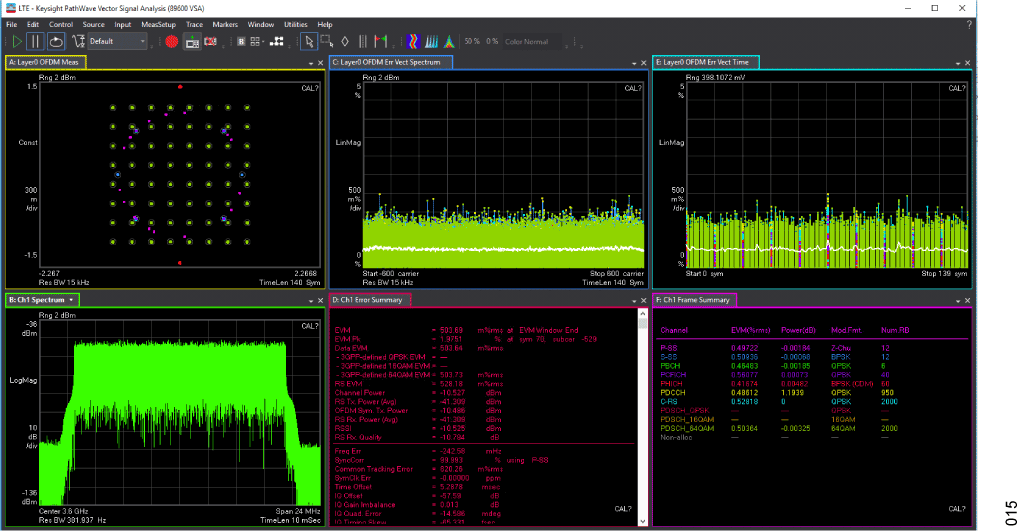
EVM is measured on a ADRV904x where four channels are toggling in TDD and FDD mode. An EVB power supply is configured in TDD mode and the channels that are running in FDD mode are measured for EVM. Results are shown in Figure 14, peak EVM of 2.3%. The board is then modified with the recommended FDD power-supply configuration. Results are shown in Figure 15, peak EVM of 1.9%. Both TDD and FDD recommended power supplies show some FDD EVM degradation during the TDD transitions. FDD solution does show slightly better performance.
If the performance in either the TDD or FDD configuration is not satisfactory, then providing a separate 1.0 V from an LDO to the balls that power the IC local oscillator synthesizers result in no EVM degradation.


LO0 is powered by: VSYN0_1P0, VDEV_1P0, VTXLO0_1P0, VLO0_1P0, VRXLO0_1P0 balls.
LO1 is powered by: VSYN1_1P0, VDEV_1P0, VTXLO1_1P0, VLO1_1P0, VRXLO1_1P0 balls.
Each set of four supply pins requires 285 mA of maximum 1.0 V supply current or both PLL0 and PLL1 sets of PLL supplies (total of seven) must be powered by an LDO for a total of 550 mA.
Recommendations for Using Ferrite Beads
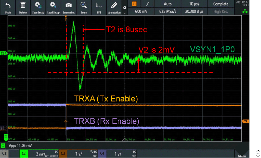
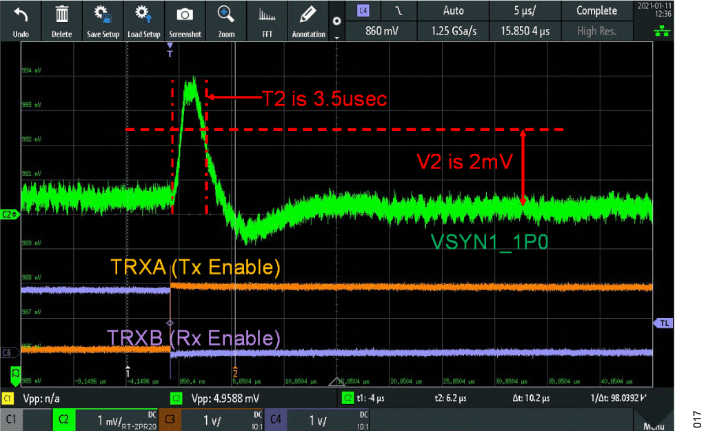
Ferrite beads are passive component that is traditionally used to suppress high-frequency signals on electronic circuit boards. The ferrite bead has an inductive response at a particular range of frequency, which effectively absorbs high-frequency transients by raising their resistance at higher frequencies. It is determined on the EVB that when operating in TDD mode that this series resonance impacts the transient response duration, which then results in higher first symbol EVM. The ferrites are removed, and the capacitors located close the IC are left in place. Characterization is done comparing receiver and transmitter spurious with and without having these beads installed. It is concluded that there are no significant differences in these spurious tests when the ferrites are removed. If the version of BOM has the ferrites installed, it is recommended to remove them when operating in TDD mode. Measured 1.0 V supply transients are provided to show the TDD response with and without the ferrite beads installed. Transmit channels are enabled as receive channels are disabled to create a TDD supply transient. Figure 16 is with ferrites beads installed it takes 8 µs (ΔT2) to settle to within 2 mV (ΔV2). And with ferrite beads removed the 2 mV time has been reduced to 3.5 µs (Figure 17).


Before adding ferrite beads to the PCB circuit, the following questions must be considered:
- What is the actual problem trying to be solved by adding ferrite bead?
- Does adding a ferrite bead solve the problem or is there a better way to solve the problem?
- The results in Figure 16 and Figure 17 show that adding ferrite beads causes a problem with power-supply transient settling. Does adding a ferrite bead cause a problem that is not existed without them?
Based upon the above questions, it is determined to remove the ferrite beads on ADRV904x EVB when operating in TDD mode. For the case of the customer system board that is operating in a noisy digital environment, it can be appropriate to add a series component shorted with a 0 Ω resistor on the power-supply pins. If the previously provided ripple specification for the power supply feeding the ADRV904x are not met, then this allows a series component to be added to solve the problem. If ferrite bead is determined to be a good solution, remember to choose a bead that is primarily resistive at the dominant noise frequencies and verify the bead DC resistance and rated current to avoid problems related to voltage drop and ferrite core saturation.