AN-1529: Extending the Dynamic Range of a 10-Bit, 65 MSPS ADC to Greater Than 100 dB Using the AD9215 High Frequency VGA
Circuit Function and Benefits
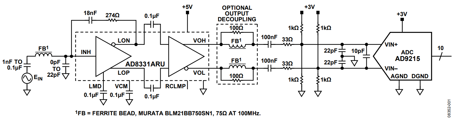
The circuit shown in Figure 1 uses the AD8331 ultralow noise, wideband variable gain amplifier (VGA) as a driver to extend the dynamic range of the AD9215 10-bit analog-to-digital converter (ADC). The gain range of the AD8331 is 48 dB and is linear in dB with respect to the control voltage. The overall dynamic range of the combined VGA and ADC is >100 dB.

VGAs serve a critical function when an analog signal with wide dynamic range is converted to digital format, and the ADC resolution is insufficient to capture all useful information. For example, a 10-bit converter with a 2 V p-p input range has an LSB weight of 2 ÷ 1024, or just under 2 mV.
This input signal represents a dynamic range of approximately 60 dB. A wideband VGA can be used ahead of the ADC to amplify input signals with amplitudes less than the minimum resolution and to attenuate large signals that otherwise saturate the ADC. An example of this kind of application is an ultrasound receiver, where the intermediate frequency (IF) amplifier is used for input signal ranges from microvolts to several volts. For dc or low frequency analog signals, Σ-Δ ADCs with resolutions of up to 24 bits are economical and plentiful; however, these ADCs are typically limited in sampling frequency to a few hundred kilohertz.
ADC resolution decreases as sampling frequency increases. This tradeoff makes accurate digitization of high frequency, low amplitude signals difficult when using standard ADCs.
VGAs are a convenient solution to this problem. The AD8331 single-channel, AD8332 dual-channel, and AD8334 quad-channel VGAs are ultralow noise and linear in dB, and are optimized for ultrasound systems. These VGAs can be used as low noise variable gain elements at frequencies up to 120 MHz.
Each channel includes an ultralow noise preamp (LNA), an X-AMP® VGA with 48 dB of gain range, and a selectable gain postamp with adjustable output limiting. The LNA gain is 19 dB with a single-ended input and differential outputs. Using a single resistor, the LNA input impedance can be adjusted to match a signal source without compromising noise performance.
The 48 dB gain range of the VGA makes the AD8331 suitable for a variety of applications. Excellent bandwidth uniformity is maintained across the entire range. The gain control interface provides precise linear in dB scaling of 50 dB/V for control voltages between 40 mV and 1 V. Factory trim ensures excellent deviceto-device and channel-to-channel gain matching.
Circuit Description
VGAs and modern ADCs have much greater functionality than the conventional op amps used with early ADC designs. In the VGA used in this circuit, gain is controlled externally. Pins are provided for selecting between gain values mapped for 10-bit or 12-bit converters, and the impedance of the low noise stage is adjustable over a wide range of impedance values with a series resistor capacitor (RC) network. The high speed converter options are available with simple pin strapping.
The circuit shown in Figure 1 demonstrates the interconnection of a typical VGA and ADC. For this example, the AD8331 VGA and AD9215 ADC are compatible in frequency range and differential interface matching. For clarity, power supply decoupling is omitted from Figure 1.
The AD8331 includes a low noise preamplifier, followed by a differential attenuator and gain stages. The AD8331 VGA requires only a single 5 V power supply. Low noise 3 V for the ADC can be provided by a low dropout (LDO) regulator, such as the ADP3339, which is connected to the 5 V supply. The differential output of the VGA is designed to drive ADCs with differential inputs over a wide range of devices from 1 V p-p to about 4.5 V p-p. The input range of the AD9215 can be set between 1 V p-p differential and 2 V p-p differential. For this circuit, the ADC input range was set to 2 V p-p differential.
The AD8331 requires an internal midsupply reference for a pair of mirrored amplifiers that provide equal but opposite polarity signals at the output referenced to the common-mode voltage. Consult the AD8331 data sheet for further information regarding this function. The VCM pin of the AD8331 functions as the common-mode voltage input and output. As an output, the VCM circuit is available for dc coupling at the VCM pin, or the pin can be driven from a voltage source to modify the value of the common-mode voltage to accommodate ADCs with various input ranges. Left floating, the VCM voltage is half of the supply voltage, which is optimum for ac-coupled applications.
The RCLMP pin clamps the output swing within the limits of the differential inputs of the ADC and avoids overdrive, which can be a serious problem with converters. A simple resistor controls the clamp amplitude (see the AD8331 data sheet for full details). If no connection is made to the RCLMP pin, the clamp voltage is 4.5 V p-p differential centered on a common-mode voltage of 2.5 V.
A 1 MHz sinewave was selected for the test waveform, and a recovered waveform from the ADC Analyzer™ software is shown in Figure 2. The sampling frequency is 65 MSPS, which corresponds to the 65 MSPS version of the AD9215.

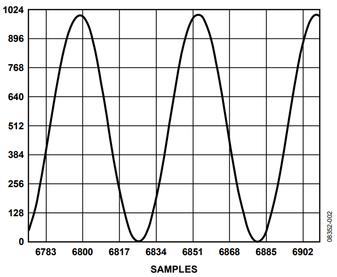
The LNA input signal was 70 mV p-p, following external lowpass and high-pass filters to reject signal generator spurs. The VGA gain was 29 dB, amplifying the signal to about half of the full-scale input voltage of the ADC. Combined high-pass and low-pass filtering between the VGA and the ADC attenuates low frequency noise below 50 kHz (33 Ω and 100 nF yield a low frequency cutoff frequency of 48 kHz) and frequencies above 100 MHz (42 pF and 33 Ω yield a high frequency cutoff frequency of 114 MHz).
Additional high-pass filtering is possible by reducing the value of the series capacitor at the LNA input and the series capacitors between the LNA and VGA inputs.
An output decoupling network, consisting of a fixed 100 Ω resistor in parallel with a ferrite bead inserted in series with each AD8331 output, can be required if there is more than approximately 25 pF of stray printed circuit board (PCB) trace capacitance on the VOH and VOL pins. Otherwise, this network is not required.
Most modern ADCs provide pin access to the internal reference. For the AD9215, the internal reference voltage is 1 V, and external resistors bias the common-mode input voltage at half of the 3 V supply.
Common Variations
Other single-channel, 10-bit ADCs include the AD9214 for lower input frequencies.
参考資料
MT-073 Tutorial. High Speed Variable Gain Amplifiers (VGAs). Analog Devices.
MT-074 Tutorial. Differential Drivers for Precision ADCs. Analog Devices.
MT-075 Tutorial. Differential Drivers for High Speed ADCs Overview. Analog Devices.
MT-076 Tutorial. Differential Driver Analysis. Analog Devices.