AN-1360: ADGM1304 および ADGM1004 は試験用計測器のチャンネル密度と試験機能をどのように向上させるか
Introduction
The AD9548 is a digital PLL with a direct digital synthesizer (DDS) as a surrogate for the VCO that appears in an analog PLL. Unlike a VCO, however, the output signal of a DDS derives from a dedicated external clock source—the system clock. The system clock is essentially the sampling clock for the DDS.
The frequency of the system clock (fS) relates to the DDS output frequency (fO) via a digital frequency tuning word (FTW) as follows:

where n is the number of bits in the DDS phase accumulator (n = 48 for the AD9548).
The AD9548 performs the PLL function by controlling FTW to produce the desired (fO) in a manner similar to the way an analog PLL varies the VCO control voltage to produce the desired VCO output frequency.
In most applications, the stability of the frequency source (the VCO in an analog PLL or the system clock in the case of the AD9548) is not of primary concern because the action of the PLL control loop tends to compensate for any intrinsic frequency drift. In applications involving a very low loop bandwidth, however, the rate of frequency drift becomes an issue because the loop may not be able to respond quickly enough to compensate when the frequency drift rate is too high. The result is a shift in phase at the output of the PLL, which can be detrimental in some critical timing applications.
One such timing application is synchronization to a 1 pps global positioning system (GPS) reference signal. These applications require loop bandwidths in the 0.02 Hz range. With such a low loop bandwidth, the intrinsic frequency drift rate of the AD9548 system clock can result in the device losing lock. This raises the question: What intrinsic frequency drift rate associated with the system clock can the AD9548 PLL tolerate without causing an adverse effect? The purpose of this application note is to provide an answer to this question.
Frequency Drift Analysis
VCO and DDS Frequency Drift Models
Because this application note focuses on the effect of system clock drift on the closed-loop operation of the AD9548 digital PLL, it makes sense to derive a model of frequency drift in an analog PLL vs. a DDS-based PLL. In an analog PLL (see Figure 1), the frequency source is a VCO. In a DDS-based PLL (see Figure 2), the frequency source is a fixed-frequency (fS) external oscillator.

Figure 1. VCO Mode.
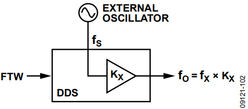
Figure 2. DDS Model.
A VCO consists of a free running oscillator that oscillates at a given nominal frequency, fC. However, the VCO is tunable over a frequency range, usually by means of a dc control voltage, VC. A model of the VCO (see Figure 1) includes the nominal frequency source, which provides the base frequency (fC), and an additional voltage-dependent frequency source associated with the frequency tunable component of the VCO. The tuning component provides a frequency offset that depends on the VCO gain (KV). Therefore, the VCO output frequency (fO) is the sum of the base and offset frequencies. Frequency drift at the VCO output (ΔfO) can result from oscillator drift (ΔfC), control drift (ΔKV), or a combination thereof.
A DDS, on the other hand, relies on an external fixed-frequency oscillator clock source that serves as the DDS sample clock and operates at a frequency of fS. A DDS model (see Figure 2) includes an input for the external sample clock, a control input (FTW) for frequency tuning, and a frequency gain element (KX).
Normally, a DDS operates under the assumption that the external sample clock frequency, fS, is a constant, stable frequency source. In this case, fX and KX in Figure 2 correspond to FTW and fS/2n in Equation 1, respectively. That is, the output frequency changes proportionally to FTW according to the frequency gain factor, KX = fS/2n.
Conversely, in the case of a nonconstant frequency source (one that exhibits drift), the previous assumption is no longer valid.Therefore, to analyze the effect of a nonconstant frequency source, assume FTW is constant. Then, fX and KX in Figure 2 correspond to fS and FTW/2n in Equation 1, respectively. That is, the output frequency changes proportionally to fS according to the frequency gain factor, KX = FTW/2n. However, Equation 1 indicates FTW/2n = fO/fS, which leads to Equation 2 implying that changes in fS translate to the output with a gain factor that is dependent upon the output frequency, fO.

where:
fO is the DDS output frequency for a given FTW.
fS is the nominal drift-free sample clock frequency.
In summary, the value of the frequency gain element in Figure 2depends on which input causes the output frequency to change. When FTW is the source of interest, then KX = fS/2n. On the other hand, when fS is the source of interest, then KX = fO/fS.
S-Domain Loop Model
Although the AD9548 is a digital PLL, the usual s-domain analysis found in the literature for analog PLLs is still applicable. Consider the block diagram in Figure 3, which is an s-domain model of the AD9548 when operating in a closed-loop configuration. A description of the various building blocks follows.

Figure 3. AD9548 s-Domain Block Diagram.
There are four terminals associated with the closed-loop configuration: IN, FB, OUT, and SYSCLK. The IN terminal constitutes the reference input signal to the phase detector of the digital PLL, while the FB terminal constitutes the feedback input. Note the negative sign at the summing junction associated with the FB input, which indicates that the feedback signal subtracts from the input signal. The OUT terminal constitutes the output of the PLL (that is, the output of the DDS in the case of the AD9548). The SYSCLK terminal is where the user connects an external clock signal, which constitutes the source of the sample clock for the DDS.
The AD9548 provides the option of multiplying the SYSCLK input frequency via an integrated system clock multiplier PLL, which is a conventional analog PLL. The scale factor, N1, in Figure 3 models the frequency multiplication effect of the system clock multiplier PLL. Although not shown explicitly in Figure 3, the system clock multiplier PLL includes a feedback divider (N), an input divider (M), and a 2× input frequency multiplier. The configuration of the system clock multiplier PLL is user programmable, which means that the value of N1 depends on the user-defined configuration according to Table 1.
| (N1) | AD9548 System Clock Multiplier Configuration |
| 1 | Bypassed |
| N/M | HF path |
| N | LF or XTAL path, 2× multiplier bypassed |
| 2N | LF or XTAL path, 2× multiplier enabled |
Note that the digital PLL shown in Figure 3 includes a feedback divider (1/N0) that divides the frequency at the OUT terminal by a factor of NN0 and delivers it to the FB terminal. The value of N0 is variable because it is a user-programmable quantity. The digital PLL also includes a phase detector with Gain KD, a loop filter with Transfer Function F(s), and a DDS with Gain KX. In keeping with the s-domain model for the gain of the VCO in an analog PLL, the DDS gain from the output of the loop filter to the DDS output is KX/s, where KX is the tuning gain (fS/2n) and the 1/s term is the Laplace operator for integration.
Response to a Linear Frequency Ramp
According to Gardner (see the References section), the transient behavior of a Type II second order PLL is also applicable to Type II PLLs beyond second order. The AD9548 is a Type II fourth-order PLL; therefore, according to Gardner’s premise, the transient behavior of a Type II second-order PLL still applies to the AD9548 even though it incorporates a fourth-order loop.
With this in mind, consider the response of a Type II second-order PLL to a linear frequency ramp at its input as shown in Figure 4. The frequency ramp has a constant slope of β (rad/sec2). The steady-state condition for a Type II second-order PLL that results from the application of a linear frequency ramp at the IN terminal is a static phase error (θe) between the IN and FB terminals.

Figure 4. Linear Frequency Ramp Input.
The static phase error resulting from an input frequency ramp is deterministic. It relates to the linear rate of frequency change (β) and the natural frequency (ωn) of the second-order loop as shown in Equation 3.

Equation 3 requires θe to have radian units. However, it is often more desirable to refer to a time offset rather than a radian phase offset, but this requires knowledge of the nominal frequency (fR) at the IN terminal. Given (fR), use Equation 4 to convert a time offset to a phase offset.

The significance of Equation 3 is that it relates a frequency ramp rate (β) at the IN terminal to a static phase offset (θe) given the natural frequency (ωn) of the loop. If a way exists to relate β at the IN terminal to the SYSCLK terminal instead, then it should lead to a method for determining the maximum tolerable linear frequency drift of the system clock source. In fact, such a relationship exists as explained in the Relating a Frequency Ramp at the IN Terminal to the SYSCLK Terminal section.
Natural Frequency
An obstacle to applying Equation 3 is the fact that the concept of natural frequency only applies to a second-order loop (a Type II PLL with a first-order loop filter, for example). This poses a problem because the AD9548 is a Type II PLL with a third-order loop filter (making it a fourth-order loop). Gardner, however, provides a means to extend the concept of natural frequency to Type II PLLs of an order greater than 2. This extension makes use of Equation 5.

where:
K is the open-loop gain.
τ2 is the time constant associated with the zero in the open-loop
transfer function.
Maximum Tolerable Frequency Ramp at the IN Terminal
According to Equation 3, the frequency ramp rate (β) at the IN terminal (see Figure 4) depends on ωn and θe. Because ωn relates to the characteristics of the loop (K and τ2 per Equation 5), its value is constant for a given PLL. On the other hand, θe depends on the slope (β) of the frequency ramp applied to the input of a Type II second-order PLL (see the Response to a Linear Frequency Ramp section). Therefore, choosing a maximum tolerable static phase offset at the input (θe) with ωn being constant establishes the maximum tolerable frequency ramp (β) at the input via Equation 3. Furthermore, Equation 4 provides a means to express θe as a time offset rather than a phase offset.
For example, consider a maximum acceptable time offset of 10 ns (Δt = 10 ns), a nominal input frequency of 1 MHz (fR = 1 MHz), and a loop natural frequency of 10 Hz (ωn = 20π rad/sec). These values result in θe = 0.06283 rad (Equation 4) and β = 39.5 Hz/sec (see Equation 3). The value given for β requires dividing the result for β in Equation 3 by 2π to convert from rad/sec2 to Hz/sec. This result implies that as long as the input frequency changes at a linear rate less than 39.5 Hz/sec, the time offset between the IN and FB terminals remains less than 10 ns.
Of course, application of Equation 3 requires a value for ωn, something that has not yet been addressed. However, Equation 5 reveals that ωn depends on K and τ2, both of which relate to the characteristics of the loop filter. Fortunately, it is possible to determine K and τ2 for the AD9548 loop filter as explained in the Determining the Natural Frequency of the AD9548 Loop Filter section.
Relating a Frequency Ramp at the IN Terminal to the SYSCLK Terminal
At this point, β (the maximum tolerable input frequency ramp rate) is quantifiable by specifying the amount of static phase (or time) offset one is willing to accept at the input (assuming one has a value for ωn). However, the goal is to determine the maximum tolerable frequency ramp at the SYSCLK terminal, not at the IN terminal. Therefore, a means of relating a frequency ramp at the IN terminal to a frequency ramp at the SYSCLK terminal must be established.
Relating a frequency ramp at the IN terminal to a frequency ramp at the SYSCLK terminal first requires a more detailed explanation of what happens within the PLL for the following two different stimuli:
- A frequency ramp at the IN terminal (see Figure 5)
- A frequency ramp at the SYSCLK terminal (see Figure 6)
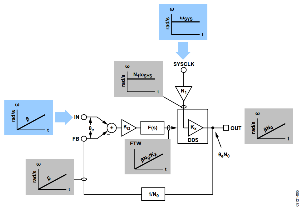
Figure 5. Frequency Ramp at the IN Terminal.
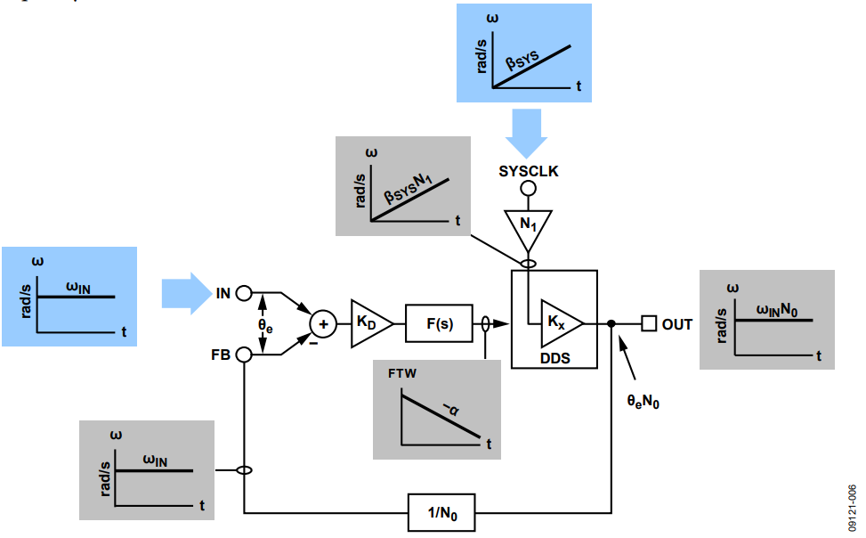
Figure 6. Frequency Ramp at the SYSCLK Terminal.
In both Figure 5 and Figure 6, the shaded rectangles are plots of frequency vs. time at various nodes in the loop, with blue denoting a stimulus signal and gray a response signal.
With a frequency ramp as the stimulus to the IN terminal (see Figure 5), note the stimulus at the SYSCLK terminal, which indicates a horizontal line (a slope of 0). This denotes a constant input frequency at the SYSCLK terminal, exactly what is expected for the system clock source. The constant frequency at the SYSCLK terminal results in a constant frequency at the output of the N1 block (the equivalent of fS in Figure 2).
The stimulus at the IN terminal is a frequency ramp with a positive slope of β, indicating a linearly increasing frequency over time. The equilibrium condition of the loop with a linear ramp at the IN terminal is a constant phase offset (θe) between the IN and FB terminals (see the Response to a Linear Frequency Ramp section).
The constant phase offset at the input of the phase detector causes a linearly increasing sequence of frequency tuning words at the output of the loop filter. Recall that the AD9548 is a digital PLL using numeric FTWs to control the output frequency of a DDS rather than a dc voltage to control the output frequency of a VCO. Therefore, the linearly ramping FTWs produce a linear frequency ramp at the OUT terminal.
The slope of the output ramp is such that it causes a replica of the ramp at the IN terminal to appear at the FB terminal (with a constant time offset defined by θe). The replicated ramp at the FB terminal is a necessary condition for equilibrium. Because the slope of the ramp at the FB terminal is β, the slope of the ramp at the OUT terminal must be βN0 due to the feedback divider. The DDS, however, has a gain of KX = fS/2n associated with its control input. Therefore, the slope of the DDS control signal necessary to produce the ramp at the OUT terminal is the slope of the ramp at the OUT terminal divided by KX as given by Equation 6.

Next, consider a frequency ramp stimulus at the SYSCLK terminal (instead of the IN terminal) as shown in Figure 6. Note the stimulus at the IN terminal, however, which indicates a horizontal line (a slope of 0). This constitutes a constant frequency at the IN terminal. In this case, a constant frequency at the IN terminal is necessary to clearly demonstrate how the loop responds to a frequency ramp stimulus at the SYSCLK terminal.
The stimulus at the SYSCLK terminal is a frequency ramp with a positive slope of βSYS, indicating a linearly increasing frequency over time. The optional system clock multiplier PLL scales the slope by a factor of N1 (see Table 1). If the loop is artificially broken at the connection between the loop filter and the DDS (simulating open-loop operation), the output signal becomes a frequency ramp with a slope of βSYS × 1 × KX, where KX is the DDS gain associated with its sample clock input according to Equation 2. Thus, in open-loop operation, the slope of the ramp at the OUT terminal is βSYS × N1 × fO/fS.
However, the fact that Figure 6 constitutes a closed loop with negative feedback means that the signal at the FB terminal must be the same as the signal at the IN terminal (a necessary condition for equilibrium). Therefore, both the IN and FB signals are a constant frequency. Furthermore, a constant frequency at the FB terminal requires a constant frequency at the OUT terminal (although scaled by the feedback divider).
To have a constant frequency at the OUT terminal, however, the control signal applied to the DDS must be a ramp with a negative slope (–α in Figure 6). In fact, the negative slope of the control signal ramp must be such that it counteracts the ramp at the output of the N1 block to yield the required constant frequency at the OUT terminal. Note that a negative sloping control signal is only possible when a constant phase offset (θe) appears between the IN and FB terminals—the equilibrium condition of a PLL in response to a frequency ramp stimulus (see the Response to a Linear Frequency Ramp section).
Recall that in open-loop operation, the DDS output signal exhibits a frequency ramp with a slope of βSYS × N1 × fO/fS. To counteract this slope, however, the control signal must operate through the FTW input of the DDS, which has a gain of KX = fS/2n. That is, α must equal the open-loop output slope (βSYS × N1 × fO/fS) divided by KX per Equation 7.

Figure 5 and Figure 6 reveal that application of a frequency ramp at the IN or SYSCLK terminal results in a pair of matching signals at the IN and FB terminals with a static phase offset (θe) between them. Furthermore, to achieve equivalence between Figure 5 and Figure 6 requires θe to be the same magnitude in both cases. This provides a link between β and βSYS via the DDS control signal. Thus, equating the magnitudes of the control ramp slopes (Equation 6 and Equation 7) establishes the necessary relationship between β and βSYS.
| βN0/(fS/2n ) | = | – (βSYSN1fO/fS)/(fS/2n)|
Solving for βSYS yields:

In Equation 8, the default units for βSYS are rad/sec2. To convert to the more familiar units of Hz/sec, use Equation 9.

Sometimes a normalized representation, like parts per million per second (ppm/sec), is more appropriate. Use Equation 10 to make the conversion.

where fSYSCLK is the nominal frequency of the source connected to the SYSCLK terminal (see Figure 3).
Determining the Natural Frequency of the AD9548 Loop Filter
Calculation of Equation 8 requires a value for β, but this, in turn, requires a value for the natural frequency of the loop (ωn) per Equation 3. Furthermore, determining a value for ωn requires knowledge of the loop filter response. In the case of the AD9548, the loop filter is a digital filter with programmable coefficients, which gives the user control over the frequency response of the loop. Because the programmed coefficients determine the loop filter response, they also determine ωn (the natural frequency of the loop).
The challenge at hand is to find a relationship between the filter coefficients and the parameters K and τ2 in Equation 5, which allows calculation of ωn. Then, substituting ωn into Equation 3 enables calculation of β, which leads to βSYS via Equation 8 (the maximum tolerable frequency drift rate of the system clock source).
The first step, however, is finding values for K and τ2, which depend on the filter response as dictated by the loop filter coefficients. The standard design procedure for calculating the AD9548 loop filter coefficients involves the six design parameters in Table 2. Note that the feedback division factor (N0) comprises an integer part, S, and an optional fractional part, U/V. Thus, the total feedback division value is S + U/V.
| Parameter | Description |
| fS | DDS sample rate (Hz) |
| fC | Desired loop bandwidth (Hz) |
| θPM | Desired phase margin |
| f3 | Frequency offset (Hz), relative to the PLL output frequency, at which the third pole response yields additional attenuation, A |
| A | Additional attenuation (dB) of the third pole response at the offset frequency, f3 |
| N0 | Feedback division factor |
The six parameters in Table 2 along with the two gain terms, KD and KV, allow for the computation of nine intermediate variables. These intermediate variables not only lead to the filter coefficients but also allow for the computation of K and τ2, which are necessary for Equation 5. The two gain terms, nine intermediate variables, and associated formulas follow:
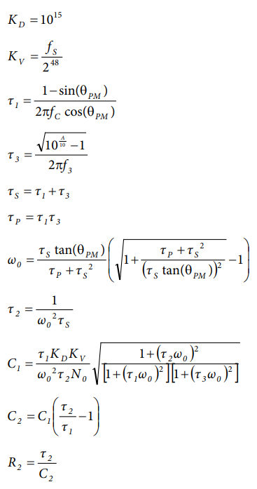
For the AD9548, the loop gain K (which is necessary to calculate ωn per Equation 5) relates to KD, KV, N0, C1, C2, and R2 as follows:

Note, however, that the equation for R2 indicates τ2 can replace C2R2 in the above equation for K. According to Equation 5, this means ωn is expressible in terms of KD, KV, N0, C1, and C2. However, C2 is proportional to C1, and the appropriate substitutions yield an alternate form for ωn according to Equation 11. The significance of Equation 11 is ωn (and by inference β) is independent of KD, KV, and N0. However, Equation 11 involves ω0, τ1, and τ3, implying that ωn is dependent on θPM, fC, f3, and A (see Table 2).

In summary, four of the six design parameters in Table 2 lead to the natural frequency (ωn) of the loop for the AD9548 via Equation 11. Insertion of ωn into Equation 3, along with the maximum acceptable phase offset (θe), yields the maximum tolerable frequency ramp rate (β) at the IN terminal. Then, β leads directly to βSYS (via Equation 8), which is the maximum tolerable frequency ramp rate at the SYSCLK terminal for a given maximum acceptable phase offset (θe) between the IN and FB terminals.
An Illustrative Example
Consider the AD9548 configured as follows:
- The reference input is a 1 Hz signal with the AD9548 input divider set to unity, resulting in a 1 Hz signal at the input to the phase detector (the IN terminal in Figure 3). Therefore,
- fR = 1 Hz
- The AD9548 SYSCLK input (the SYSCLK terminal in Figure 3) is a 25 MHz oscillator and uses the HF path of the integrated system clock multiplier PLL (see Table 1.) to generate a 1 GHz system clock. Therefore,
- fSYSCLK = 25 MHz
- N1 40 (N1 = N/M, where N = 40 and M = 1)
- fS = 1 GHz
- With the AD9548 in closed-loop operation, the DDS output frequency is (155,520,000 + 185/188) MHz. Therefore,
- S = 155,520,000
- U = 185
- V = 188
- N0 = S + U/V = 155,520,000 + 185/188
- fO = (155,520,000 + 185/188) Hz
(because fO = fR × N0)
- The loop filter has the following parameters (see Table 2):
- fC = 0.02 Hz
- θPM = 60°
- f3 = 1 Hz
- A = 15 dB
- The maximum acceptable time offset at the phase detector input (the IN and FB terminals in Figure 3) is 1 ns. Therefore,
- Δt = 1 ns
These parameters yield:
τ1 = 2.13227
τ3 = 8.80729 × 10⁻¹
ω0 = 8.77306 × 10⁻²
The values of τ1, τ3, and ω0 enable calculation of ωn via Equation 11 (note τS = τ1 + τ3).
ωn = 4.47996 × 10⁻²
Use Equation 4 to convert Δt to θe.
θe = 2πfRΔt = 6.28319 × 10⁻⁹
Use Equation 3 to calculate β from ωn and θe.
β = θe(ωn)2 = 1.26104 × 10⁻¹¹ (rad/sec2)
Use Equation 8 to calculate βSYS.
βSYS = β(N0/N1)/(fO/fS) = 3.15259 × 10⁻⁴ (rad/sec2)
Use Equation 9 and/or Equation 10 to convert to Hz/sec and/or ppm/sec.
βSYS (Hz/sec) = 5.02 × 10⁻⁵
βSYS (ppm/sec) = 2.01 × 10⁻⁶
The significance of this result cannot be overemphasized—the maximum rate of change of frequency at the SYSCLK terminal for this example is a mere 50 μHz/sec. Because the nominal SYSCLK frequency for this example is 25 MHz, 50 μHz/sec translates to 2 micro-ppm/sec or 2 milli-ppb/sec (ppb is parts per billion).
Choosing the Proper SYSCLK Source
For the specific case given in the An Illustrative Example section, the maximum tolerable rate of change of frequency at the SYSCLK terminal is 2 milli-ppb/sec, which implies the need for an extremely stable SYSCLK source to maintain a time offset (Δt) of no more than 1 ns.
Consider a SYSCLK source, for example, consisting of a very high quality 25 MHz OCXO capable of providing temperature stability in the range of 2 ppb/°C. Suppose such an OCXO experiences a 10°C temperature change over the course of an hour. Assuming that the temperature change (δT/δt) is constant over the one-hour interval, the frequency shift is:
2 ppb/°C × 10°C/hour = 5.6 milli-ppb/sec
This is 2.8 times greater than the 2 milli-ppb/sec maximum tolerable rate of change of frequency for the example given in the An Illustrative Example section. For that particular case, there are three ways to deal with this problem of an excessive frequency drift rate.
- Choose an environment that keeps the temperature change to about 3.5°C/hour (instead of 10°C/hour).
- Choose an OCXO with a temperature stability specification of no more than 0.7 ppb/°C.
- Increase θe or ωn, or a combination of both, to increase β by a factor of 2.8, thereby increasing βSYS to 5.6 milli-ppb/sec (commensurate with the OCXO drift rate).
Considering the third option, it may be possible to increase the Δt requirement from 1 ns to 2.8 ns because Δt equates to θe (Equation 4) and θe is directly proportional to β (Equation 3), which is directly proportional to βSYS (Equation 8). However, if changing Δt is not feasible, ωn could be increased instead.
This, however, is a much more difficult option for two reasons. First, rather than β being directly proportional to ωn, it is proportional to its square. Second, ωn depends on the loop filter response, which relates to the parameters in Table 2. This makes the relationship between ωn and the loop filter response quite convoluted.
Normalization Helps Quantify SYSCLK Stability Requirement
As a guide to assist in choosing an appropriate SYSCLK source, Figure 7 and Figure 8 offer a link between acceptable time offset (Δt), open-loop bandwidth (fC in Table 2), and the maximum tolerable frequency ramp at the SYSCLK terminal (βSYS). Both figures cover a range of fC from 0.001 Hz to 0.1 Hz with βSYS given in normalized units of ppm/sec. The use of normalized units allows for more meaningful plots because it masks the effect of N0, N1, fO, and fS on βSYS (see Equation 8).

Figure 7. θPM = 50°.

Figure 8. θPM = 80°.
To benefit from normalization, however, requires a constant attenuation factor (parameter A in Table 2). To this end, all plot traces are for A = 3 dB. Normalization also requires the offset frequency (parameter f3 in Table 2) to scale with fC by a constant factor, which is the case for all plot traces. However, to capture the effect of changing the relative position of f3, each Δt value comprises two traces—a black trace corresponding to f3 = 20×fC (a scale factor of 10) and a red trace corresponding to f3 = 20×fC (a scale factor of 20).
Comparison of the two figures reveals that a particular Δt trace in Figure 7 (θPM = 50°) results in a higher βSYS value relative to the same Δt trace in Figure 8 (θPM = 80°). This implies a less stringent stability requirement on the SYSCLK source for a lower θPM value. Furthermore, the separation between red and black traces for a given Δt value seems to indicate that higher θPM values are more sensitive to the location of f3. For example, Figure 7 (θPM = 50°) reveals about a 25% increase in βSYS when scaling f3 by a factor of 20 (red trace) vs. a factor of 10 (black trace). This suggests there is a slightly less stringent requirement on the stability of the SYSCLK source for f3 scaled by 20 vs. 10 given θPM = 50°. On the other hand, Figure 8 (θPM = 80°) reveals about a 100% increase in βSYS when scaling f3 by a factor of 20 (red trace) vs. a factor of 10 (black trace). This implies a factor-of-two less stringent stability requirement on the SYSCLK source for f3 scaled by 20 vs. 10 given θPM = 80°.
Conclusion
Using the AD9548 to generate an output clock signal synchronized to a 1 pps GPS reference signal requires a very low loop bandwidth (0.02 Hz, for example). A very low loop bandwidth results in a similarly low natural frequency.
The low natural frequency combined with the requirement of a stringent time offset (Δt) leads to a very small value for βSYS (the maximum tolerable rate of change in frequency at the SYSCLK terminal for which the loop can maintain a time offset of Δt or less). Finally, the very small βSYS value implies the need for an extremely stable SYSCLK source. Thus, it requires great care in choosing the appropriate SYSCLK source when employing very narrow loop bandwidths.
Methodology Caveats
The method described herein for establishing a value for β and applying Equation 8 allows for quantifying βSYS. The value of βSYS represents the maximum rate of change of frequency at the SYSCLK terminal of the AD9548 that results in a phase (or time) offset of no more than θe (or Δt) given a particular device configuration.
Keep in mind that the maximum tolerable linear drift rate of frequency indicated by βSYS relies on the following assumptions:
- The frequency drift is of constant slope (δf/δt = constant) and persists long enough for the loop to reach equilibrium (steady-state condition).
- Using the s-domain model for an analog PLL is sufficiently accurate for modeling the behavior of the AD9548.
- The transient behavior of a second-order loop is sufficiently similar to that of higher order loops, which justifies the use of Equation 3.
- The extended definition of natural frequency, as proposed by Gardner, justifies the use of Equation 5.
The implication of these assumptions is that the calculated value of βSYS is an estimate of the maximum tolerable frequency drift, rather than a hard boundary condition.
Regarding the Loop Bandwidth of the System Clock Multiplier PLL
Some applications involve the use of the AD9548’s integrated system clock multiplier PLL to translate a relatively low frequency SYSCLK source to a frequency high enough to accommodate the DDS. Such was the case demonstrated in the An Illustrative Example section. When the system clock multiplier PLL is in use, its bandwidth has a potential effect on a frequency ramp (βSYS) appearing at the SYSCLK terminal. Fortunately, the bandwidth of the system clock multiplier PLL is so wide relative to the slow frequency ramps under consideration in this application note, the impact of its loop response on determining βSYS is inconsequential.
はじめに
このアプリケーション・ノートでは、ADGM1304 およびADGM1004 マイクロマシン(MEMS)スイッチと、これらのスイッチが試験装置アプリケーション、特に自動試験装置(ATE)アプリケーションにもたらすメリットについて説明します。MEMS スイッチは、RF リレーと比較して、サイズ上のメリット、広帯域の無線周波数(RF)性能、高精度の DC/0 Hz 性能、そして機械的な動作寿命が長いというメリットを有しています。これらは ATE アプリケーションにおいて重要なものです。
ここでは、基板面積の削減と性能向上の観点から、どこにMEMS スイッチを使用できるか、そして一般的に使用されている RF リレーに比べて MEMS スイッチが有用な場所はどこかを代表的なシグナル・チェーンとブロック図で示します。また、このアプリケーション・ノートでは、試験装置に使用される標準的なリレーの性能と MEMS スイッチの性能を比較して説明します。
試験用計測器におけるスイッチング
背景
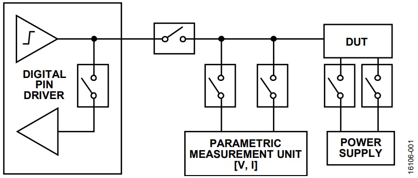
スイッチ機能は、あらゆる電子テスト用計測器において基本的で重要な機能です。テスト対象デバイス(DUT)がますます複雑さを増し、チャンネル/ピン数や機能も増えつつあるのに伴い、必要な試験の種類と回数も増加してきました。高精度の DC電圧および電流特性試験、ミックスド・シグナル試験、高周波デジタル試験、そして RF 試験のすべてが 1 つのデバイス評価で行われる可能性があります。そして、多くの場合、それらの試験は並行して行われます。特に自動試験装置(ATE)では 1 つのデバイス評価に数百回もの試験が必要となるため、試験のスピードが重要です。使用する試験の種類と信号が複雑になると、試験用ハードウェアのアーキテクチャとそれに使用するスイッチ機能にも影響が及びます。ATE 試験用計測器による代表的な試験セットアップの概略的なブロック図を図 1 に示します。これは一般的に見られるもので、デジタル・ピン・ドライバ、パラメトリック計測ユニット(PMU)、電源が、ATE 試験装置内の 1 枚の計測器試験カードに集積され関連し合ってスイッチングを行います。

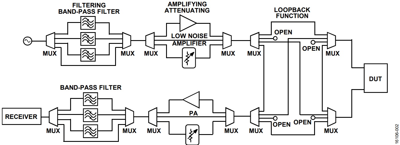
補助的なスイッチング機能も試験装置の外部、特にデバイス・インターフェース・ボード(DIB、試験インターフェース・ユニット(TIU)と呼ばれることもある)上で必要とされることがあります。図 2 に、DUT の AC/RF 試験用にセットアップした DIB の機能およびスイッチ構成例を示します。ノイズ・フロアの最小化やプリント回路基板(PCB)の損失低減など、試験システムの性能向上に十分な柔軟性を持たせるため、多くの場合、DUT の試験ボードには信号のフィルタリング、アンプ、およびキャリブレーションで構成されたパスが必要となります。

使用するスイッチの種類は、試験に必要な信号の種類と性能で決まります。現在の試験装置とデバイス用 TIU 基板には、相補型金属酸化膜半導体(CMOS)スイッチ、光 MOS スイッチ、リード・リレー、電子機械式リレー(EMR)スイッチ、ガリウム・ヒ素(GaAs)ベースの RF スイッチ、およびシリコン・オン・インシュレータ(SOI)ベースの RF スイッチが使用されています。
多くの高性能ソリッドステート・スイッチが ATE 試験装置に使用されていますが、PMU の DC 信号や高速のデジタル/RF 信号を最小限の信号損失と歪みで共通の試験用信号経路に印加しなければならない場合は、未だにサイズの大きな EMR が使用されています。このような試験条件は高性能電子デバイスの試験では一般的です。RF デバイスや高速のデジタル・デバイスでは、多くの場合、膨大な回数の高精度 DC 電圧および電流試験、高速デジタル・インターフェース試験、および RF 信号の送受信試験が行われています。PMU による高精度の試験は、一般的にDUT のリーク特性評価を目的に行われ、高速計測と組み合わせることでデバイス性能に関する重要な結果が得られます。高精度な試験と高速の試験に対する要求から、高性能 EMR の使用が加速されることになります。
しかし、EMR には制約もいくつかあります。制約には、大きい、動作が遅い、サイクル寿命がきわめて限られている、配線上の問題から PCB の設計が難しい、高出力の外部ドライバ回路が必要、リワークが難しい、などが挙げられます。使用する EMR が、大型かつ同軸コネクタ・タイプでモジュラー型のフォーム・ファクタを持つものでないとしても、EMR は帯域幅が限られているため、実現できるシステム性能とシステムのチャンネル数が大きく制約される可能性があります。
MEMS スイッチの利点
MEMS 技術
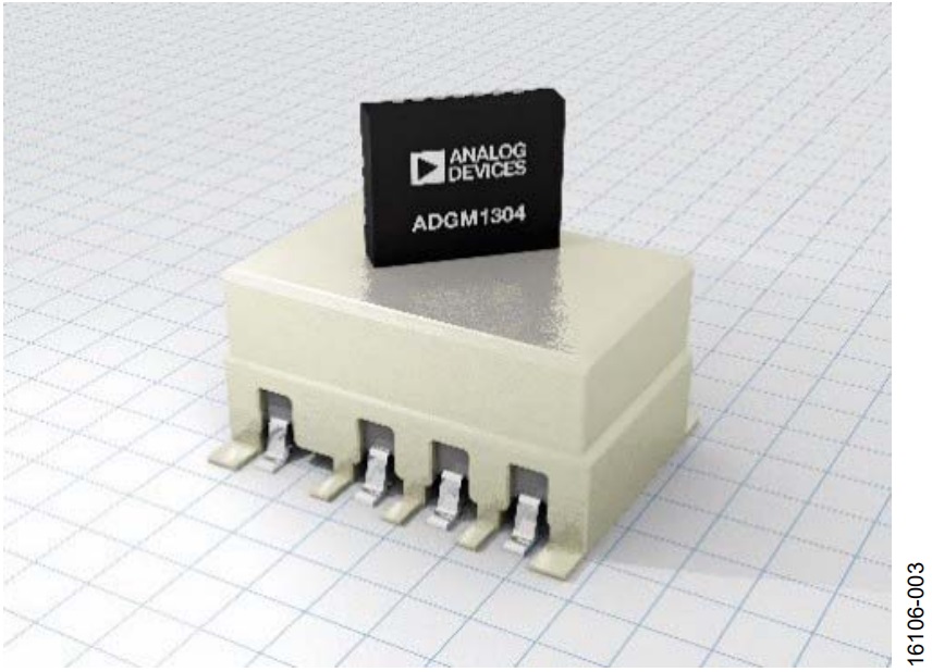
アナログ・デバイセズの MEMS スイッチは、EMR のメリットを非常に小型のフォーム・ファクタに集積するとともに、RF 性能とサイクル寿命を向上させています。MEMS スイッチ技術の詳細については、技術資料のアナログ・デバイセズの革新的MEMS スイッチ技術の基礎を参照してください。試験用計測器ではスイッチのサイズが非常に重要で、試験用計測ボードやDUT のインターフェース用 TIU ボードで実現可能な機能とチャンネル数がこれによって決まります。図 3 に、0 Hz/DC ~14 GHz、単極 4 投(SP4T)MEMS スイッチの ADGM1304 を、標準的な 3 GHz 帯域幅、2 極双投(DPDT)EMR の上に載せた状態で示します。体積にすると 90 % 以上のサイズ低減を達成できます。

MEMS 技術による物理的なサイズのメリットに加えて、このスイッチは電気的および機械的性能でも大きなメリットを有しています。表 1 に、ADGM1304 および ADGM1004 デバイスの主な仕様を、標準的な高周波、単極双投(SPDT)8 GHz EMR と比較して示します。ADGM1304 および ADGM1004 デバイスは、帯域幅、挿入損失、スイッチング時間に優れているとともに、10億サイクルのサイクル寿命を実現しています。高い帯域幅は、スイッチの用途を新しいアプリケーション領域に拡大する場合に重要です。電源を内蔵した低消費電力、低電圧のドライバを搭載していることも MEMS スイッチの重要な利点です。ADGM1004 は、人体モデル(HBM)で 2.5 kV、電界誘起帯電デバイス・モデル(FICDM)で 1.25 kV の高い静電放電(ESD)定格を備えており、使いやすさをさらに向上させています。
| Switch Parameter | ADGM1304 MEMS | ADGM1004 MEMS | 8 GHz EMR (Typical) |
| Switch Configuration | SP4T | SP4T | SPDT (1 Form C) |
| Operational Frequency (3 dB) | 0 Hz/dc to 14 GHz | 0 Hz/dc to 13 GHz | 0 Hz (dc) to 8 GHz |
| LFCSP Size | 4 mm × 5 mm × 0.95 mm | 4 mm × 5 mm × 1.45 mm | 8.0 mm × 9.4 mm (TO-5) |
| On Resistance (RON) | 1.6 Ω (typical) | 1.8 Ω (typical) | 0.15 Ω (maximum) |
| On Leakage | 5 nA | 5 nA | 5 nA |
| Actuation Lifetime | 1 billion cycles (minimum) | 1 billion cycles (minimum) | 10 million cycles (typical) |
| Switching Speed | 30 μs (typical) | 30 μs (typical) | 4 ms (maximum) |
| Power Supply | 3.3 V (10 mW = 3.3 V x 2.9 mA), integrated driver | 3.3 V (10 mW = 3.3 V x 2.9 mA), integrated driver | 5 V (280 mW), external driver required |
| Insertion Loss (IL) | 0.4 dB (typical) at 6 GHz | 0.6 dB (typical) at 6 GHz | 0.8 dB (typical) at 6 GHz |
| Off Isolation | 24 dB (typical) at 2.5 GHz | 24 dB (typical) at 2.5 GHz | 27 dB (typical) at 3.0 GHz |
| Power Rating | 36 dBm, ±6 V dc | 32 dBm, ±6 V dc | 1 Amp/28 V dc |
| ESD Rating, RF Ports (HBM; FICDM) | 100V; 500V | 2.5 kV; 1.25 kV | Not specified |
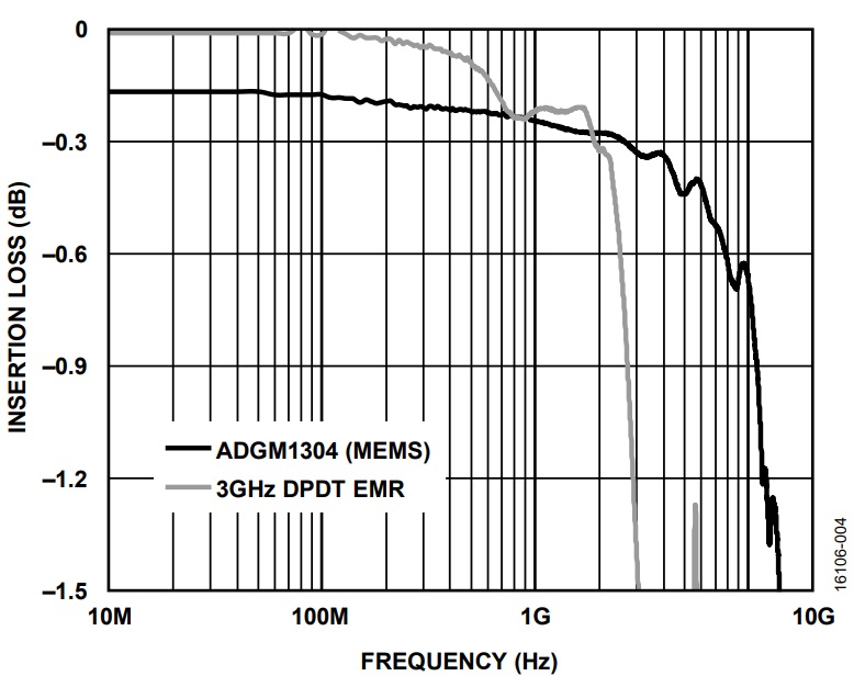
図 4 に、ADGM1304 SP4T MEMS スイッチの挿入損失とオフ・アイソレーションを、試験用計測器で一般的に使用されているDPDT 3 GHz EMR と比較して示します。図 4 から、EMR よりMEMS スイッチのほうが信号帯域幅に優れていることがわかります。

MEMS スイッチのアプリケーション例
従来、ATE 試験装置で DC/RF スイッチ機能を実現するためには EMR スイッチは欠かせないものです。しかし、リレーを使用すると、以下の問題のためにシステム性能が制限されることがあります。
- リレー・スイッチのサイズが大きく、設計ルールに禁止エリアを設けなければならないため、非常に大きな面積が必要で試験の拡張性に欠ける。
- リレーのサイクル寿命が限られており、通常は数百万 ~ 数千万サイクルしかない。
- 所望のスイッチ構成を実現するには、複数のリレーをカスケード接続する必要がある(例えば、SP4T 構成には 3 個のSPDT リレーが必要)。
- PCB 実装の問題として、多くの場合、リレーを使用するとPCB のリワーク率が高くなる。
- 配線の制約とリレー性能の限界により、完全な帯域幅性能を実現するのが非常に困難な場合がある。
- リレーの動作速度がミリ秒単位と遅いため、試験のスピードが制限される。
図 5 から図 7 に、ATE アプリケーションにおいて MEMS スイッチがどのようにこれらの制約に対処し、価値を高めることができるかを示します。EMR スイッチを使用した場合と ADGM1304または ADGM1004 MEMS スイッチを使用した場合の、代表的なDC/RF スイッチのファンアウト・アプリケーションの回路図を図 5 と図 6 に示します。図 7 に、この 2 つの回路図から作製したデモ用 PCB の写真を示します。このデモ用 PCB では、ファンアウトによる 16:1 のマルチプレクサ機能が使用されています。図 5 で使用するリレーは DPDT EMR リレーです。18:1 のマルチプレクサ機能を実現するには、9 個の DPDT リレーと 1 個のリレー・ドライバ IC が必要です(8 個の DPDT リレーでは 14:1 のマルチプレクサ機能しか得られません)。物理的なリレー・ソリューションを図 7 の基板の左側に示します。この写真から、リレー・ソリューションが大きな面積を占めること、対称性のある配置で実装するのが難しいこと、そしてドライバ IC が必要であることがわかります。

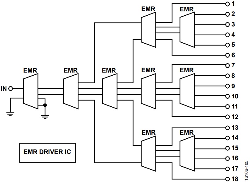
図 6 と、図 7 の基板の右側に、同様のファンアウト・スイッチ機能をわずか 5 個の ADGM1304 または ADGM1004 SP4T MEMSスイッチによって簡略化したものを示します。この 2 つの図から、スイッチ機能が占める PCB 面積と配線の複雑さが低減していることがわかります。x-y 面積にして 68 % 以上、体積にすると 95 % 以上の削減が可能です。ADGM1304 および ADGM1004 MEMS スイッチには独立にスイッチを制御できる低電圧ドライバが内蔵されているため、外部ドライバ IC は不要です。MEMSスイッチはパッケージの高さが低いため(ADGM1304 が 0.95mm、ADGM1004 が 1.45 mm)、スイッチを PCB の裏面にも実装できます。これにより、チャンネル密度をさらに向上させることが可能です。

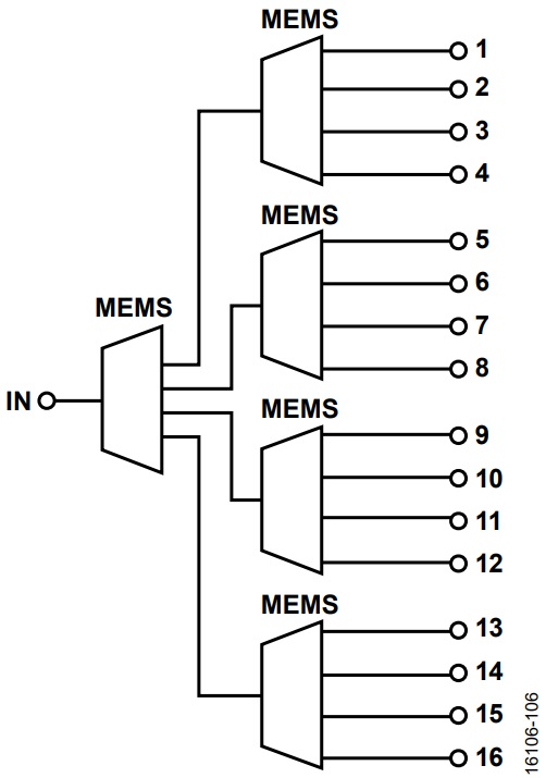

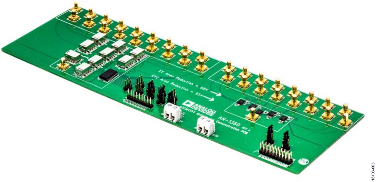
図 8 に試験装置におけるスイッチの使用例をもう 1 つ示します。この図は、高速または RF DUT に接続する試験用インターフェースのスイッチに EMR を使用した場合の、代表的な回路図を示しています。この場合、電子デバイスを評価するために高速のRF 信号とデジタル/DC 信号の両方が必要です。

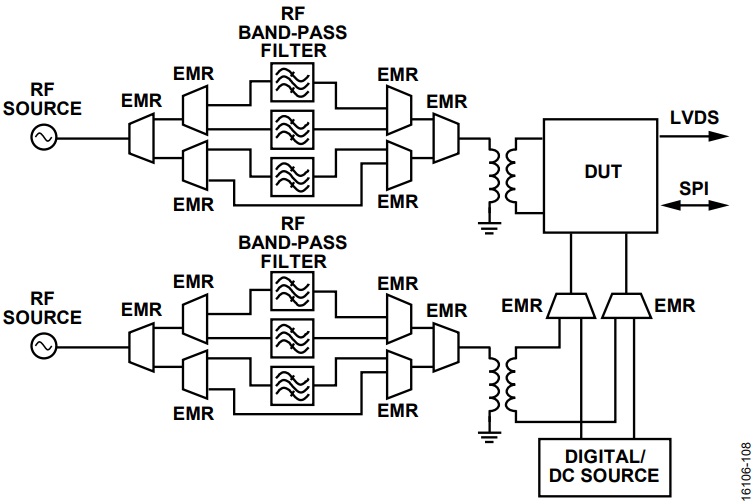
図 8 では、スイッチ・ソリューションとしてリレーを使用しています。バンドパス・フィルタの選択、デジタル信号のルーティング、DC のパラメトリック試験機能を実現するには、14 個の SPDT リレーが必要です。リレーは、カスケード接続しなければなりません。
MEMS スイッチを使用した等価なソリューションを図 9 に示します。図 9 は、MEMS スイッチを使用することで試験インターフェースの設計の簡略化と機能向上が実現できることを表しています。この設計は、わずか 6 個の ADGM1304/ADGM1004 しか必要としないため、

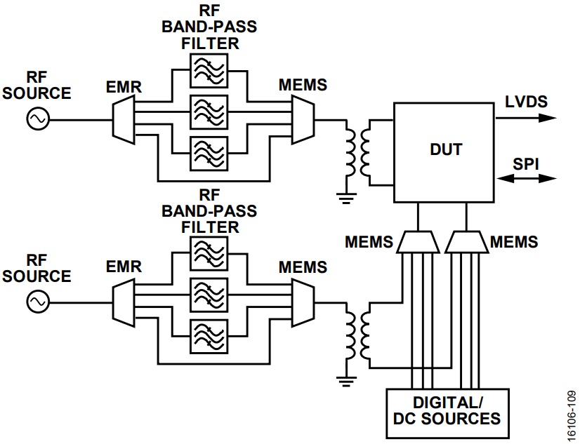
配線の複雑さと基板面積を大幅に削減できます。ADGM1304 と ADGM1004 スイッチは SP4T 構成のため、デジタル/DC パラメトリック試験機能にリレーを使用した場合に 4 チャンネルになるのに対して、MEMS スイッチでは 8 チャンネルを確保できます。これにより、全体でより多くの機能チャンネルが得られます。14 GHz の広帯域幅、0 Hz/DC 動作、小型パッケージ・サイズ、そして低電圧制御が可能なこの MEMSスイッチは、高い柔軟性、長いサイクル寿命、小面積のスイッチ・ソリューションを可能にするとともに、高精度かつ高速のデジタル信号ルーティングと広帯域 RF 信号ルーティングを同時に実行できます。
まとめ
デバイスの複雑さが増し、試験条件が拡大したため、ATE ソリューションの性能およびスペース効率の最適化が困難になっています。スイッチは、DC/デジタルおよび RF 機能が要求される今日のあらゆる ATE 試験ソリューションにおいて不可欠な部品です。アナログ・デバイセズの MEMS スイッチ技術は、試験機能および性能の向上と、従来の RF リレー・ソリューションに比べて小さい PCB 面積を実現できる独自の技術です。ADGM1304 および ADGM1004 は高精度 DC 性能と広帯域 RF 性能を備えた SP4T MEMS スイッチで、小型の SMD パッケージに収容されており、低い駆動電力条件、長いサイクル寿命、高 ESD 耐性を可能にします。これらの機能により、アナログ・デバイセズの MEMS スイッチ技術はあらゆる最新 ATE 装置に最適な汎用スイッチ・ソリューションとなっています。
参考資料
Analog Devices Makes MEMS Switch Technology a Commercial Reality. Analog Devices Product Highlight. 2017.
Carty, Eric. アナログ・デバイセズが実現した MEMS ベースの RF スイッチ技術 Video. Analog Devices. 2016.
Carty, Eric and McDaid, Padraig. 革新的な 5 KV ESD MEMS スイッチ技術 Technical Article. Analog Devices. 2017.
Carty, Eric, Fitzgerald, Padraig, and McDaid, Padraig. アナログ・デバイセズの革新的 MEMS スイッチ技術の基礎 Technical Article. Analog Devices. 2016.
著者