資料ライブラリ
AN-1066: Power Supply Considerations for the AD9523, AD9524, and AD9523-1 Low Noise Clock
Introduction
This application note is a guide to help users understand how the design of the power supply management can affect the performance of the Analog Devices, Inc., AD9523, AD9524, and AD9523-1 family of low noise and low power clock products. Also described are the details of the system board layout and frequency planning.
The AD9523, AD9524, and AD9523-1 clock products offer an alternative single-chip solution with superior integration, performance, and power consumption characteristics.
In all applications, the clock products require 1.8 V and 3.3 V supplies. Various noise and coupling scenarios must be considered during system board design to ensure that all noise and spurious impact are understood.
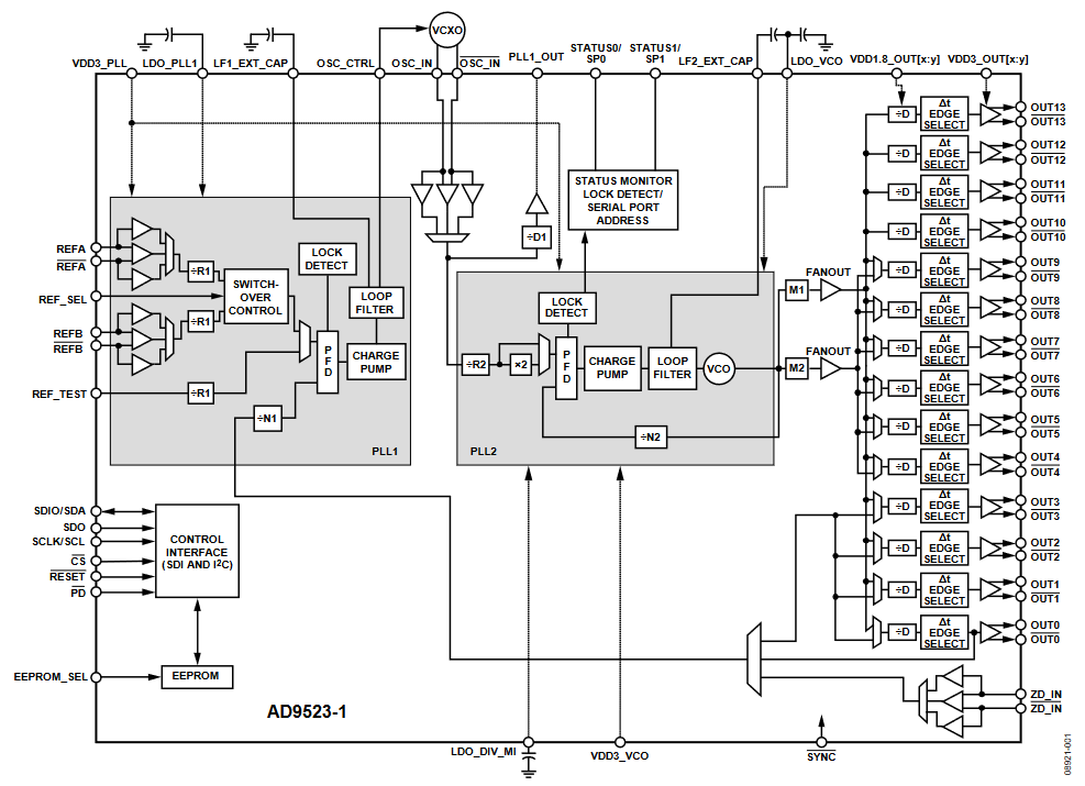
Figure 1. AD9523-1 Top Level Diagram.
Noise Source Basics
Noise sources can be grouped into one of two categories: intrinsic circuit device noise and external interference. Circuit noise is common to all integrated circuit designs and includes sources such as thermal noise, flicker noise, and shot noise. External interference source examples include power supply noise and electromagnetic interference. This application note focuses on external noise sources of power supply noise and noise associated with coupling from one clock output to another.
Power Supply Noise
Power supply rejection (PSR) is how well a circuit rejects ripple coming from the input power supply at various frequencies. This is very critical to maintain the very low noise and spurious performance that is required in many RF and wireless applications. In the case of an analog-to-digital converter (ADC) clock application, amplitude noise (AM) is not as critical to the encode clock of an ADC because the sampling occurs at the clock edge. In this case, clock jitter or phase noise is the dominant cause of reduced ADC performance (see the AN-756 Application Note, Sampled Systems and the Effects of Clock Phase Noise and Jitter). However, if AM noise is converted to PM noise (time jitter), the ADC performance is degraded. For this reason, when referring to PSR in this application note, it is the measure of rejection of AM-to-PM conversion.
To measure the PSR of the circuit power supply, an ac signal is placed on the dc power pin, and the spur that is generated is measured at the clock output. This ac signal generates an AM-to-AM, AM-to-PM, or a combination of both at the clock output. As previously mentioned in the case of an ADC, it only responds to phase noise. If using a spectrum analyzer to measure the spurious signal, there is no easy way to determine if the spurious tone is AM or PM. Either a limiting amplifier is required before the spectrum analyzer or an ADC can be used to measure the clock spurious. The spurious signal is a measure of the output phase noise generated from the amplitude input ripple over a wide frequencyrange (10 Hz to 10 MHz is common) and is expressed in decibels (dBc/V rms). The data illustrated in Figure 2 is the amount of phase noise (spurious) specified in dBc/Hz vs. per 1 V rms of sinusoidal tone on each of the power supplies of a 122.88 MHz clock signal.
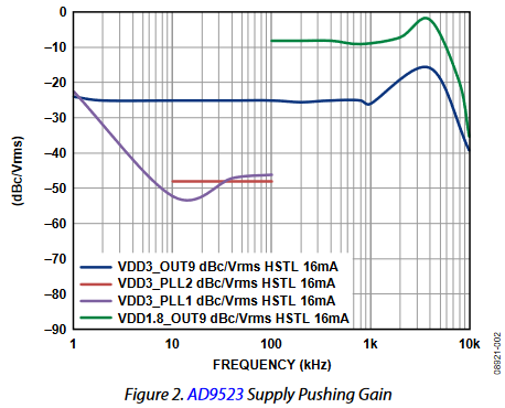
Figure 2. AD9523 Supply Pushing Gain.
Following is an example of how to derive the low dropout regulator (LDO) noise requirements for the VDD3_OUT[x:y] supply (other supply pins are done similarly).
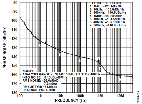
Figure 3. AD9523-1 Phase Noise, Output = 122.88 MHz (VCXO = 122.88 MHz, Crystek VCXO CVHD-950); Doubler On.
From Figure 3, the 100 kHz offset phase noise is −137.7 dBc/Hz. To only impact the phase noise by 0.5 dB, the noise due to power supply must be at least 10 dB below or −147.7 dBc/Hz. From Figure 2, there is 25 dB of internal power supply rejection of the VDD3_OUT9 supply pin. Therefore, the phase noise on this pin can be −147.7 dBc/Hz − (−25 dBc V rms) = 10(−122.7 dBrms/20) = 0.7 µV rms at 100 kHz offset.
Table 1 lists typical phase noise requirements for either the VCXO sent to any of the outputs or the standard PLL2 sent to the outputs. Noise specification for the supply pins were then generated using the method described previously. The results are listed in Table 2 through Table 5.
| Freq (kHz) | VCXO at Output (dBc/Hz | Clock at Output (dBc/Hz) |
| 1 | −128 | −123 |
| 10 | −140 | −135 |
| 40 | −145 | −137 |
| 100 | −148 | −139 |
| 800 | −156 | −156 |
| Supply Characteristics: VDD3.3_PLL1 | Limit | Unit |
| Noise Spectral Density at 1 kHz | ||
| VCXO | 8 | µV/√Hz max |
| Clock | 14 | µV/√Hz max |
| Noise Spectral Density at 10 kHz | ||
| VCXO | 59 | µV/√Hz max |
| Clock | 105 | µV/√Hz max |
| Noise Spectral Density at 100 kHz | ||
| VCXO | 12 | µV/√Hz max |
| Clock | 33 | µV/√Hz max |
| Noise Spectral Density at 800 kHz | 2 | µV/√Hz max |
| Output Ripple from 1 kHz to 60 MHz | 6 | mV p-p max |
| Supply Characteristics: VDD3.3_PLL2 | Limit | Unit |
| Noise Spectral Density at 1 kHz | 40 | µV/√Hz max |
| Noise Spectral Density at 10 kHz | 48 | µV/√Hz max |
| Noise Spectral Density at 100 kHz | 17 | µV/√Hz max |
| Noise Spectral Density at 800 kHz | 2 | µV/√Hz max |
| Output Ripple from 1 kHz to 60 MHz | 16 | mV p-p max |
| Supply Characteristics: VDD1.8_OUT[x:y] | Limit | Unit |
| Noise Spectral Density at 1 kHz | ||
| VCXO | 359 | nV/√Hz max |
| Clock | 638 | nV/√Hz max |
| Noise Spectral Density at 10 kHz | ||
| VCXO | 90 | nV/√Hz max |
| Clock | 160 | nV/√Hz max |
| Noise Spectral Density at 100 kHz | ||
| VCXO | 32 | nV/√Hz max |
| Clock | 91 | nV/√Hz max |
| Noise Spectral Density at 800 kHz | 18 | nV/√Hz max |
| Output Ripple from 1 kHz to 60 MHz | 0.26 | mV p-p max |
| Supply Characteristics: VDD3.3_OUT[x:y] 14 Outputs | Limit | Unit |
| Noise Spectral Density at 1 kHz | ||
| VCXO | 2.5 | µV/√Hz max |
| Clock | 4.5 | µV/√Hz max |
| Noise Spectral Density at 10 kHz | ||
| VCXO | 0.7 | µV/√Hz max |
| Clock | 1.2 | µV/√Hz max |
| Noise Spectral Density at 100 kHz | ||
| VCXO | 0.25 | µV/√Hz max |
| Clock | 0.8 | µV/√Hz max |
| Output Ripple from 1 kHz to 60 MHz | 2 | mV p-p max |
Figure 4 contains two phase noise traces of a 122.88 MHz clock output. One trace has elevated noise in the region of 10 kHz from the other. This due to the 1.8 V output supply noise being too high. The other trace that is lower in this region is measured while using an Analog Devices ADP150 1.8 V linear regulator as the output supply.
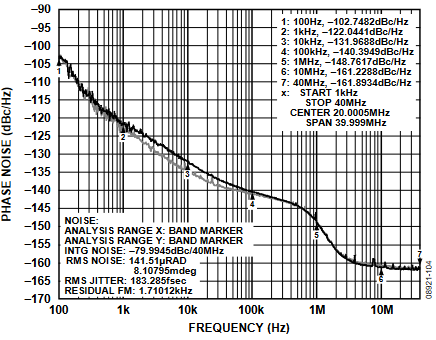
Figure 4. Example of Power Supply Noise Causing Noise.
Power Supply Configuration
Figure 5 illustrates the various power supply connections for the AD9523. Notes provide information to what circuit blocks are powered from each supply pin and how interaction of various supply domains may cause spurious signals.
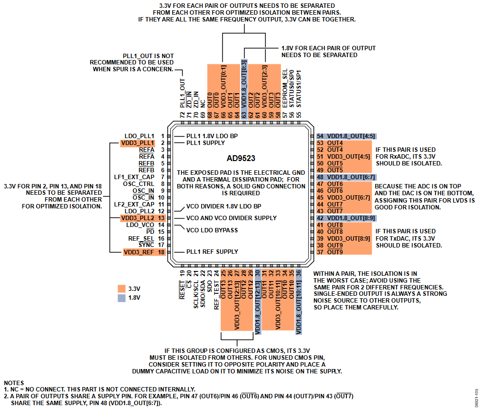
Figure 5. Power Supply Connections of the AD9523.
Figure 6 illustrates the power supply routing of the output channel circuit blocks of the AD9523. The same routing applies for the AD9524, minus OUT6 through OUT13. Figure 7 is for the AD9523-1. These figures are used to illustrate the sources of channel-to-channel coupling, which consist of the following:
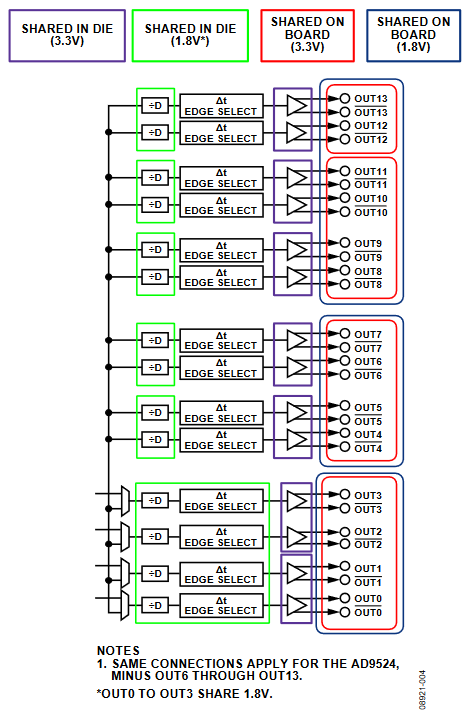
Figure 6. Output Driver Power Supply Connections of the AD9523.
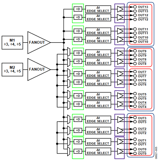
Figure 7. Output Driver Power Supply Connections of the AD9523-1.
- Shared supplies (dividers/drivers)
- Package (bond wire proximity)
- Evaluation board (traces/terminations)
- Voltage controlled oscillator (VCO) dividers (supplies/muxes pertain to the AD9523-1 dual dividers
The green, bordered areas in Figure 6 and Figure 7 highlight sections of the output channels that share the same 1.8 V and 3.3 V supply connection. The connections are in pairs and for this reason have the highest coupling to each other.
The red and blue circles highlight how the supply domains are shared on the evaluation board.
How to Interpret Table 6 and Table 7
On the left most column of Table 6 and Table 7 are the measured outputs with a clock frequency of 245.76 MHz. Across the top of Table 6 and Table 7 lists another output configured for 15.68 MHz, referred to as the aggressor. Each one of these outputs was turned on in LVPECL mode one at a time while at the same time having one aggressor turned on. The highest spurious level was recorded as a result of either the sum or the difference of the measured channel and the aggressor. The level of the spur was divided into three different categories to illustrate the coupling mechanism.
Category H is the highest category. An H occurs whenever the aggressor shares the same 3.3 V and 1.8 V on the die. Nothing can be done externally to the part to reduce this coupling. Proper frequency planning by putting the same frequency on these outputs eliminates coupling.
Category M is the moderate category. An M occurs whenever the VDD1.8_OUT supply is located between the measured output and the aggressor, for example, measuring OUT10 with the aggressor on OUT9. These outputs do not share the 3.3 V and 1.8 V supplies on the die, but the 1.8 V supply for Channel 10 is located directly beside the aggressor, OUT9.
Category L is the lowest category. An L occurs whenever the measured channel supply is from the aggressor. Proper frequency planning is achieved by placing channels such that their sum and difference frequency fall outside the band of the measured frequency.
One method to lower the coupling is to use the lowest output amplitude possible for each of the outputs. For example, when a low noise critical output is operating in LVPECL mode, configure an aggressor channel to operate in LVDS mode. The simple fact that LVDS has less ac voltage swing lowers the coupling.
In Table 6 and Table 7, observe Row OUT5 and Column OUT8, listed as L. In this case, the 3.3 V and 1.8 V supplies are separated on the AD9523, and only the 1.8 V domain is shared on the board.
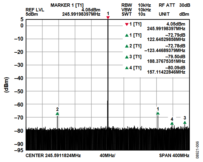
Figure 8. OUT5 with Aggressor OUT8.
| Measured Outputs (245.76 MHz) | Aggressor (15.68 MHz | |||||||||||||
| OUT0 to OUT3 | OUT4 to OUT9 | OUT10 to OUT13 | ||||||||||||
| 3.3 V and 1.8 V On Chip | 3.3 V and 1.8 V On Chip | 3.3 V and 1.8 V On Chip | 3.3 V and 1.8 V On Chip | 3.3 V and 1.8 V On Chip | 3.3 V and 1.8 V On Chip | 3.3 V and 1.8 V On Chip | ||||||||
| OUT0 | OUT1 | OUT2 | OUT3 | OUT4 | OUT5 | OUT6 | OUT7 | OUT8 | OUT9 | OUT10 | OUT11 | OUT12 | OUT13 | |
| OUT0 | N/a | H | M | M | L | L | L | L | L | L | L | L | L | L |
| OUT1 | H | N/a | M | M | L | L | L | L | L | L | L | L | L | L |
| OUT2 | M | M | N/a | H | L | L | L | L | L | L | L | L | L | L |
| OUT3 | M | M | H | N/a | L | L | L | L | L | L | L | L | L | L |
| OUT4 | L | L | L | L | N/a | H | M | M | L | L | L | L | L | L |
| OUT5 | L | L | L | L | H | N/a | M | M | L | L | L | L | L | L |
| OUT6 | L | L | L | L | M | M | N/a | H | M | M | L | L | L | L |
| OUT7 | L | L | L | L | M | M | H | N/a | M | M | L | L | L | L |
| OUT8 | L | L | L | L | L | L | M | M | N/a | H | L | L | L | L |
| OUT9 | L | L | L | L | L | L | M | M | H | N/a | L | L | L | L |
| OUT10 | L | L | L | L | L | L | L | L | M | M | N/a | H | M | M |
| OUT11 | L | L | L | L | L | L | L | L | M | M | H | N/a | M | M |
| OUT12 | L | L | L | L | L | L | L | L | L | L | M | M | N/a | H |
| OUT13 | L | L | L | L | L | L | L | L | L | L | M | M | H | N/a |
| 1 L means lowest coupling, M means moderate coupling, H means highest coupling. 2 N/a means not applicable |
||||||||||||||
| Measured Outputs (245.76 MHz) | Aggressor (15.68 MHz | |||||||||||||
| OUT0 to OUT3 | OUT4 to OUT7 | OUT8 to OUT9 | OUT10 to OUT13 | |||||||||||
| 3.3 V and 1.8 V On Chip | 3.3 V and 1.8 V On Chip | 3.3 V and 1.8 V On Chip | 3.3 V and 1.8 V On Chip | 3.3 V and 1.8 V On Chip | 3.3 V and 1.8 V On Chip | 3.3 V and 1.8 V On Chip | ||||||||
| OUT0 | OUT1 | OUT2 | OUT3 | OUT4 | OUT5 | OUT6 | OUT7 | OUT8 | OUT9 | OUT10 | OUT11 | OUT12 | OUT13 | |
| OUT0 | N/a | H | M | M | L | L | L | L | L | L | L | L | L | L |
| OUT1 | H | N/a | M | M | L | L | L | L | L | L | L | L | L | L |
| OUT2 | M | M | N/a | H | L | L | L | L | L | L | L | L | L | L |
| OUT3 | M | M | H | N/a | L | L | L | L | L | L | L | L | L | L |
| OUT4 | L | L | L | L | N/a | H | M | M | L | L | L | L | L | L |
| OUT5 | L | L | L | L | H | N/a | M | M | L | L | L | L | L | L |
| OUT6 | L | L | L | L | M | M | N/a | H | M | M | L | L | L | L |
| OUT7 | L | L | L | L | M | M | H | N/a | M | M | L | L | L | L |
| OUT8 | L | L | L | L | L | L | M | M | N/a | H | L | L | L | L |
| OUT9 | L | L | L | L | L | L | M | M | H | N/a | L | L | L | L |
| OUT10 | L | L | L | L | L | L | L | L | M | M | N/a | H | M | M |
| OUT11 | L | L | L | L | L | L | L | L | M | M | H | N/a | M | M |
| OUT12 | L | L | L | L | L | L | L | L | L | L | M | M | N/a | H |
| OUT13 | L | L | L | L | L | L | L | L | L | L | M | M | H | N/a |
| 1 L means lowest coupling, M means moderate coupling, H means highest coupling. 2 N/a means not applicable |
||||||||||||||
VCO Divider M1 and M2 Coupling (AD9523-1 Only)
The AD9523-1 offers two parallel VCO dividers to provide additional frequency planning and flexibility. The outputs from the VCO dividers, M1 and M2, couple to each other to some degree. Table 8 and Table 9 provide the amount of couple that can be expected for each divider setting. The tables have the following conditions:
- They list the highest mixing product (m × ωc ± n × ωm) between M1 and M2 dividers in an 800 MHz span.
- The numbers below spur levels are the spur frequency offsets from the carrier.
- The numbers below the divisors are the output frequencies of the dividers.
- M1 mixes onto M2 more than M2 does onto M1.
Spurs are present on both sidebands, but Table 8 and Table 9 list only the highest spurs in an 800 MHz span (carrier ± 400 MHz).
Therefore, for some divider settings, the actual aggressor frequencies happen to fall just outside of this span. For example, when M2 = ÷3, its output is roughly 1 GHz, and when M1 = ÷5, its output is roughly 600 MHz. If given a channel being driven by M2 (1 GHz) and let M1 be the aggressor (600 MHz), coupling spurs pop up at ±200 MHz while only one of the ±400 MHz spurs is visible within the 800 MHz span. The 600 MHz aggressor frequency (fc − 400 MHz) is present at −56.7 dBc, but it is not the highest spur measured. Instead, a different mixed product at −54.9 dBc was recorded in Table 9 and that happened to be +200 MHz offset from the carrier. Table 8 and Table 9 list all possible combinations of VCO divider settings and the respective coupling between them. The measurements were completed with both PLLs unlocked (pump up), and no other frequencies present on the board. A free running VCO essentially drives the VCO dividers such that the only spurs present on the spectrum are those of the VCO dividers coupling to one another.
| Measured VCO Divider (M1) | AD9523-1 VCO DIV Coupling—Aggressor (M2) | ||
| ÷3, 996.6 MHz | ÷4, 746.6 MHz | ÷5, 597.0 MHz | |
| ÷3, 996.6 MHz | −72.3, 333.46 MHz | −57.3, 250.0 MHz | −64.1, 200 MHz |
| ÷4, 746.6 MHz | −68.4, 250 MHz | −73.6, 250 MHz | −73.1, 300 MHz |
| ÷5, 597.0 MHz | −67.6, 200 MHz | −63.2, 150 MHz | −75.4, 400 MHz |
| Measured VCO Divider (M2) | AD9523-1 VCO DIV Coupling—Aggressor (M1) | ||
| ÷3, 996.6 MHz | ÷4, 746.6 MHz | ÷5, 597.0 MHz | |
| ÷3, 996.6 MHz | <−80, no spurs | −54.9, 250 MHz | −54.9, 200 MHz |
| ÷4, 746.6 MHz | −60.8, 250 MHz | −76.8, 250 MHz | −58.7, 150 MHz |
| ÷5, 597.0 MHz | −58.1, 200 MHz | −62.1, 150 MHz | <−80, no spurs |
Example Output-to-Output Coupling Considerations
This section considers the AD9523-1 configuration for a 4Rx/4Tx radio implementation. The required frequencies are summarized in Table 10.
| No. of Required Frequencies | Function | Frequency (MHz) |
| 2 | Two dual Rx ADCs, 14-bit, IF 140 MHz | 184.32 |
| 4 | Two dual Tx DACs, 14-bit, IF 140 MHz | 983.04 |
| 2 | CPRI™ | 122.88 |
| 4 | LO reference | 61.44 |
| 2 | Tx digital predistortion (DPD) ADC 12-bit | 245.76 |
Each of the required clocks has different noise and spurious requirements. Typically, the Rx ADC and Tx digital-to-analog converter (DAC) have the lowest noise and spurious requirements. Both are 14 bits that produce a very low signal-to-noise ratio (SNR) of approximately 76 dB, and there is no additional filtering in this part of the signal chain to remove any clock spurious.
The CPRI clock specification typically has a noise and spurious requirement specified in the range from 12 kHz to 20 MHz offset. Therefore, coupling from other clock outputs outside of this range may not be of concern.
The LO reference clocks at 61.44 MHz are references for other local oscillators in the system. The bandwidths of these PLLs are often designed to be 50 kHz. The response of the LO PLL is that of a high order low-pass filter, and spurs on the 61.44 MHz reference are filtered by this response. Therefore, spurs on the 61.44 MHz clocks that are >10 MHz offset are attenuated.
The Tx DPD ADC clocks at 245.76 MHz are used in the digital predistortion system. The ADC has two fewer bits than the Tx DAC or Rx ADC, making it approximately 12 dB less sensitive to noise and spurs.
Select VCO Frequency and VCO Divider
The highest required frequency is 983.04 MHz. This implies a VCO frequency of 2949.12 MHz with a VCO division of 3. An Rx ADC frequency of 184.32 MHz is not an integer division of 983.04 MHz. Therefore, both M1 and M2 VCO dividers are required. Setting the other VCO divider to 4 produces a frequency of 737.28 MHz, and a channel division of 4 produces the required 184.32 MHz for the Rx ADC.
A VCO divider of 3 and a VCO divider of 4 are needed. Refer to Table 8 and Table 9 to determine which divider, M1 or M2, must be set to ÷3 or ÷4. Table 11 lists a summary of spurious levels of all the different combinations of ÷3 and ÷4 at M1 and M2 outputs.
| Measured | Aggressor | Spur (dBc) | From Table |
| M1 ÷ 3 | M2 ÷4 | −57.3 | Table 8 |
| M1 ÷ 4 | M2 ÷3 | −68.4 | Table 8 |
| M2 ÷ 3 | M1 ÷4 | −55.9 | Table 9 |
| M2 ÷ 4 | M1 ÷3 | −60.8 | Table 9 |
The summary shows that when M1 is set to ÷4 and M2 is set to ÷3, the coupling spur is the lowest of −68.4 dBc at 250 MHz offset. However, before choosing this combination, the final required frequency must be considered. The spurious levels listed in Table 8 and Table 9 are measured at the VCO divider output frequency (channel divider = 1). The VCO divider output is divided down by any further channel division. Using this scenario of M1 set to ÷4, the 737.28 MHz output of M1 must be further divided by 4 to produce the final frequency of 184.32 MHz. This means that the −68.4 dBc spur on a 737.28 MHz carrier is now reduced by 12dB to −80.4 dBc on the 184.32 MHz clock.
20 × log(chdiv = 4)
where chdiv is the channel divider.
For the case of an M2 output of 983.04 MHz, if a Tx IF of 140 MHz is used, the spur is scaled by 17 dB.
20 × log(983.04 MHz/140 MHz)
See the AN-756 Application Note for further details on how clock spurs and noise affect the ADC noise. Because Table 8 and Table 9 list only the highest spur, any other VCO coupling spur is lower than the spurious levels listed in Table 8 and Table 9. For this example, M1 is set to ÷4 and M2 is set to ÷3.
Assign Frequency to Output Channel
The next step is to assign each frequency to an output channel. The first consideration is to group the same frequencies on the outputs that share 3.3 V and 1.8 V internal supply domains. This means OUT0 and OUT1, OUT2 and OUT3, OUT4 and OUT5, OUT6 and OUT7, OUT8 and OUT9, OUT10 and OUT11, and OUT12 and OUT13 are all pairs. The second consideration is the location of the aggressor to the shared 1.8 V supply. For example, OUT13 and OUT12 share the same 1.8 V supply, but OUT11 is adjacent to VDD1.8_OUT[12:13].
For the case of the ADC and DAC, Figure 9 can be used to determine how a clock spurious can alias into the band of interest. For the example of the Rx ADC, fS = 184.32 MHz, the IF of 140 MHz is in Zone 2, and the IF input aliases to 44.32 MHz. A clock spur is located on the IF at the same offset as on the clock. The location of where it aliases can be determined based on Figure 9. Choose the coupling spur with the least amount of impact from the aliasing effects of the ADC and DAC.
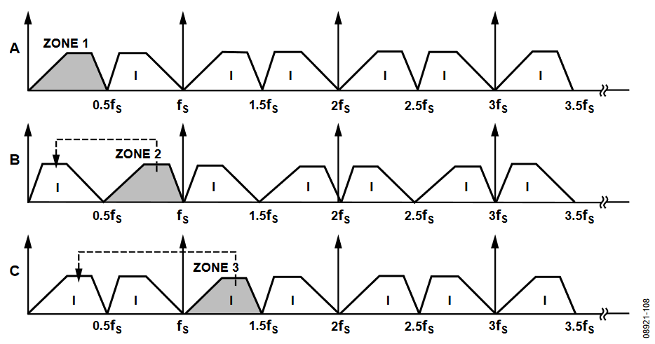
Figure 9. Undersampling Nyquist Zones.
Figure 10 shows the FFT results of the Rx ADC when all AD9523-1 outputs are running, as configured in Figure 11. The IF frequency is 44 MHz as expected. There are worst other spurs at 78 MHz and 17 MHz at −78 dBFs. As previously calculated, a spur occurs at the difference between the frequencies of the VCO divider outputs: 983.04 MHz − 737.28 MHz = 245.76 MHz. To determine the location on the FFT of the ADC, find the location of the spurious 140 MHz ± 245.76 MHz. One spur is at 385.76 MHz, which is in Nyquist Zone 5 and is located at 385.76 MHz − 368.64 MHz = 17 MHz. The other spur falls in Zone 2 and aliases to 78.5 MHz. The spurious locations match what was measured in Figure 10.
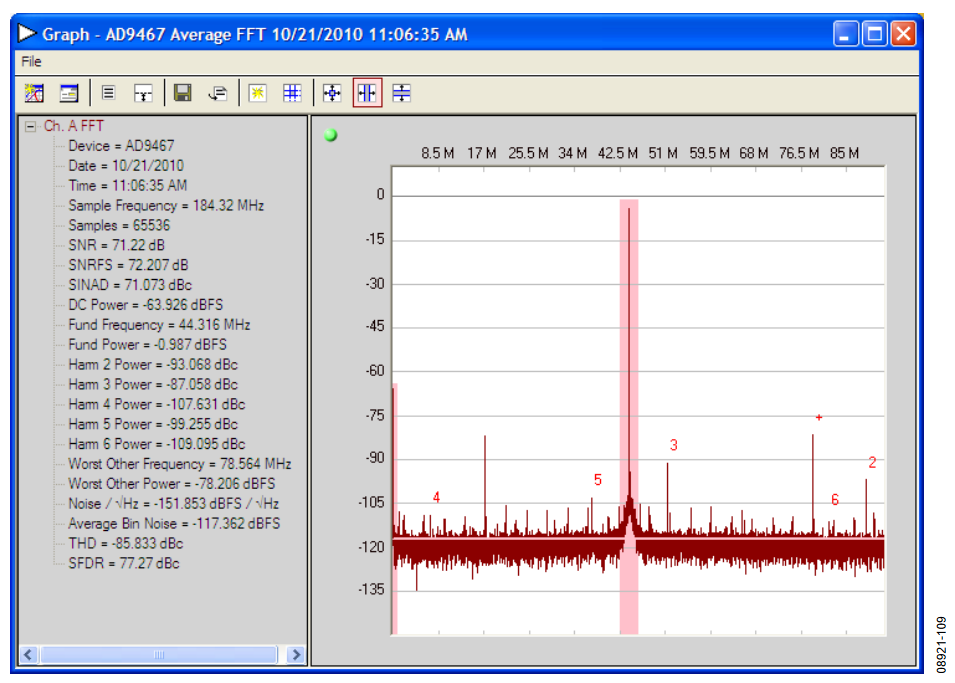
Figure 10. ADC FFT fIN = 140 MHz, fCLOCK = 184.32 MHz.
The remaining 61.44 MHz and 122.88 MHz clocks are such a large offset from the 983.04 MHz that neither clock has any impact on the system. Figure 11 illustrates the final AD9523-1output frequency configuration.
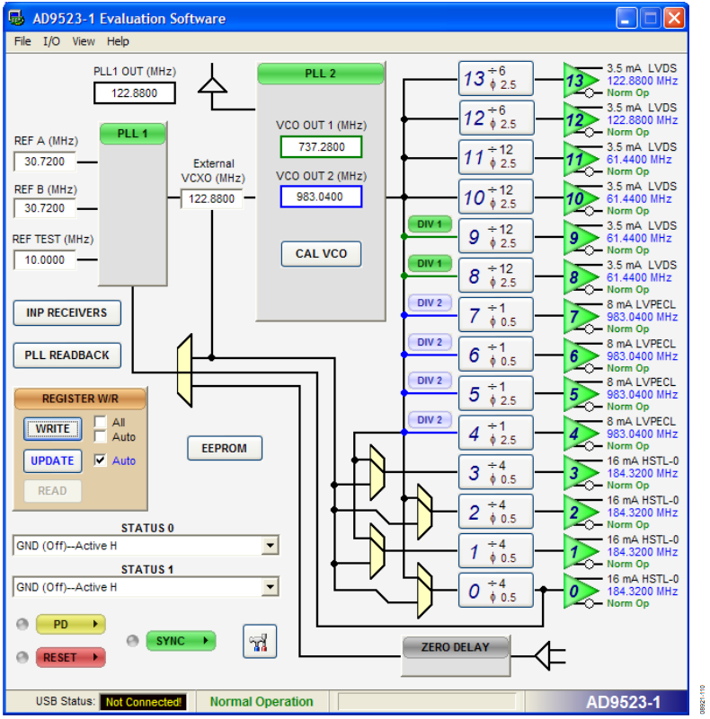
Figure 11. AD9523-1 Example Output-to-Output Coupling Considerations.
