AN-047: How to replace DRV8824 by TMC2224
The TMC220x and TMC222x family offers a pin- and package-compatible upgrade path for a number of commodity step and direction drivers. It provides superior microstepping capabilities and stealthChop™ for smooth and noiseless running motors. Additionally, the TMC2224 offers more flexibility in settings and adds advanced current control and diagnostics plus remote control via a simple-to-use UART interface. This application note shows how to replace the DRV8824 in an existing application.
Compatibility
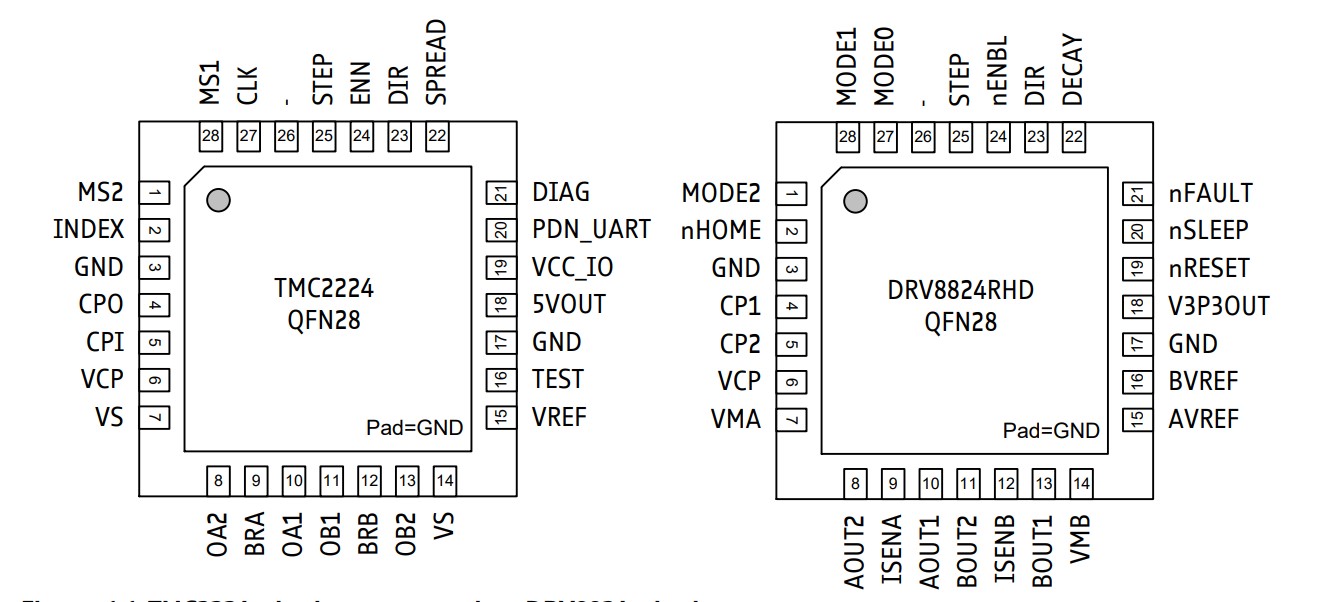
The TMC2224-LA is fully footprint compatible to the DRV8824RHD. The pinning is designed in a way that it will directly work in most applications. However, certain pins have alternate functionality, in order to optimally enhance the driver flexibility and feature set. Further, some electrical characteristics are different in order to support the architecture of the TMC2224.
Pinning Comparison

Figure 1. TMC2224 pinning compared to DRV8824 pinning.
| TMC2224 | Pin | DRV8824 | TMC2224 function | DRV8824 function | Differences |
| CLK | 27 | MODE0 (pd) | CLK input. Tie to GND or VCC for internal clock. | Microstep resolution setting | Identical for most common microstep settings. See Table 1.1. Do not leave CLK pin floating. |
| MS1 (pd) | 28 | MODE1 (pd) | Microstep resolution setting | ||
| MS2 (pd) | 1 | MODE2 (pd) | |||
| INDEX | 2 | nHOME | High active push/pull index output. | Low active open drain index output. | If used, invert software function. |
| GND, pad |
3, 17 |
GND | - | ||
| CPO | 4 | CP1 | External 22nF charge pump capacitor | External 10nF charge pump capacitor | Assemble different value capacitor. |
| CPI | 5 | CP2 | |||
| VCP | 6 | Tie to VS using 100nF capacitor. | Tie to VS using 100nF capacitor and 1MΩ resistor. | - (Save a resistor.) |
|
| VS | 7, 14 |
VMA VMB |
- | ||
| OA2 | 8 | AOUT2 | - | ||
| BRA | 9 | ISENA | - | ||
| OA1 | 10 | AOUT1 | - | ||
| OB1 | 11 | BOUT1 | - | ||
| BRB | 12 | ISENB | - | ||
| OB2 | 13 | BOUT2 | - | ||
| VREF | 15 | AVREF | Reference voltage for current scaling. | Slightly different scaling. Adapt voltage or sense resistor value. | |
| TEST | 16 | BVREF | May alternatively be connected to VREF. | Normally tied to AVREF. | |
| 5VOUT | 18 | V3P3OUT | Output of 5V regulator. Use 2.2µF to 4.7µF capacitor to GND. | Output of 3.3V regulator. Use 0.47µF capacitor to GND. | Assemble different value capacitor. |
| VCC_IO | 19 | nRESET (pd) | 3.3V to 5V IO supply voltage for all digital pins. | Normally high Reset pin. Pull to GND to reset the IC. | No change, if directly connected to logic high level voltage. |
| PDN_UART (pd) | 20 | nSLEEP (pd) | Power down input: Logic low enables automatic standstill current reduction. Optional UART I/O. | Sleep control input: Logic high enables the driver, logic low disables it. | No change, unless TMC2224 automatic current reduction or UART is used. |
| DIAG | 21 | nFAULT | High active push/pull level upon driver error. | Low active driver error output. | If used, invert software function. |
| SPREAD (pd) | 22 | DECAY (pu&pd) | Chopper mode: Low=stealthChop, High=spreadCycle |
Decay mode: Low=slow, Open=mixed, High=fast |
No change, unless it is desired to change mode. |
| DIR (pd) | 23 | DIR (pd) | - | ||
| ENN (pd) | 24 | nENBL (pd) | - | ||
| STEP (pd) | 25 | STEP (pd) | - | ||
| N.C. | 26 | N.C. | - | ||
Summary of major differences
Microstep Setting
The TMC2224 uses two pins for setting four different microstep resolutions, while the DRV8824 uses a third pin adding three settings. On the TMC2224, the third pin is an optional-use clock input, which might be tied high or low for normal operation. Additional microstep settings from fullstep up to 256 microsteps are possible via the serial interface. In this case, the pin setting has no influence. The most important settings share a common configuration (see Table 2).
| TMC2224 MS2 DRV8824 MODE2 |
TMC2224 MS1 DRV8824 MODE1 |
TMC2224 CLK DRV8824 MODE0 |
TMC2224 function | DRV8824 function |
| 0 | 0 | 0 | ¼ step | fullstep |
| 0 | 0 | 1 | ¼ step | ½ step |
| 0 | 1 | 0 | 1/8 step | ¼ step |
| 0 | 1 | 1 | 1/8 step | 1/8 step |
| 1 | 0 | 0 | 1/16 step | 1/16 step |
| 1 | 0 | 1 | 1/16 step | 1/32 step |
| 1 | 1 | 0 | 1/32 step | 1/32 step |
| 1 | 1 | 1 | 1/32 step | 1/32 step |
nHOME (INDEX) and nFAULT (DIAG) Output
The TMC2224 uses push/pull output stages rather than open drain output. This will save external pull-up resistors, but polarity has been inverted. Inverting the polarity easily is done in software. While these outputs rarely are used in stepper applications, differences will not impact most applications. However, it is not possible to tie outputs in parallel.
nRESET (VCC_IO) Input
While the DRV8824 has a dedicated reset input, the TMC2224 uses a dedicated I/O voltage supply on the same pin. As the nRESET input has to be tied to the positive I/O voltage for normal operation, this pin directly is suited to supply the I/O drivers, without any change in the schematic. However, no series resistor should be used in this pin connection.
In applications where a reset is desired, the TMC2224 also can be reset by driving VCC_IO pin to GND. Make sure that all input signals are driven to GND at the same moment, because they would try to keep up the power supply via the ESD protection input diodes.
External Capacitors
The driver requires a number of external capacitors for charge pump and internal voltage regulator. Capacity values are different for the TMC2224. The slightly larger values for the charge pump capacitor (22nF recommended) and the linear regulator output capacitor (2.2µF recommended) help reducing motor noise and power dissipation.
AVREF/BVREF (VREF) input respectively Sense Resistor
Both ICs set the basic motor current by a sense resistor. The current defined by the sense resistor can be scaled via an analog input (AVREF and BVREF, resp. VREF). To yield the same motor current with the TMC2224, a slightly different combination of VREF voltage and sense resistor value is required. In applications where VREF is used for scaling, it is most easy to adapt VREF for fine-tuning, e.g., by poti or software PWM.
DRV8824:

VREF range is 0 to 4V.
TMC2224:

VREF range is 0 to 2.5V. VREF > 2.5V gives the same result at 2.5V.
Application Example
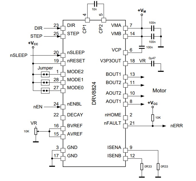
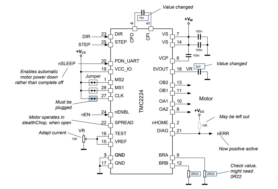
The following schematic shows a typical application example (Figure 2a) and the adaptation of component values when dropping-in TMC2224 (Figure 2b).

Figure 2a. DRV8824 application schematic.

Figure 2b. Upgrade by TMC2224 (blue: values requiring modification).
Disclaimer
ADI TRINAMIC Motion Control GmbH & Co. KG does not authorize or warrant any of its products for use in life support systems, without the specific written consent of ADI TRINAMIC Motion Control GmbH & Co. KG. Life support systems are equipment intended to support or sustain life, and whose failure to perform, when properly used in accordance with instructions provided, can be reasonably expected to result in personal injury or death.
Information given in this application note is believed to be accurate and reliable. However no responsibility is assumed for the consequences of its use nor for any infringement of patents or other rights of third parties which may result from its use.
Specifications are subject to change without notice.
All trademarks used are property of their respective owners.
参考資料
TMC222x_TMC222x_Datasheet, www.analog.com
