A 16-bit 16-MS/s SAR ADC With On-Chip Calibration in 55-nm CMOS
A 16-bit 16-MS/s SAR ADC With On-Chip Calibration in 55-nm CMOS
I. INTRODUCTION
Successive approximation register (SAR) ADCs have gained considerable research interest over the past decade or so [1]-[9]. The relatively simple architecture due to hardware reuse without requiring operational amplifiers (opamps) makes it more power efficient and easier to port between processes. Furthermore, the supply voltage scaling in advanced CMOS processes has less of a toll on SAR ADCs because the comparator only requires a small output swing to distinguish decisions from noise. This is unlike the opamps in pipelined ADCs or sigma-delta ADCs where reduced supply voltage translates to much lower opamp output swing due to fixed circuit overhead voltage drop, which leads to much decreased ADC signal to noise ratio (SNR).
One of the performance spaces that SAR ADCs excel at is high resolution at relatively low speed. They find many applications ranging from medical imaging, instrumentation, to industrial process control, etc. Compared to sigma-delta ADCs, which are also well suited in the low speed space, SAR ADCs distinguish themselves with the capability of converting one sample at a time, among others. Furthermore, SAR ADCs better handle multiplexed inputs compared to incremental sigma-delta ADCs especially when only lower oversampling ratio (OSR) is allowed, and SAR ADCs do not require much signal post-processing.
Typically, precision SAR ADCs [3], [4], which are generally defined at 16-bit and greater, sample at below a few MS/s. A few works [1], [2] have pushed the speed further. They use 2-bit/trial and the pipelined SAR architecture [7], [10] to speed up the operation, at the cost of added design complexity and a high accuracy amplifier. In addition, these ADCs typically have a sampling capacitance larger than 20 pF to achieve more than 90-dB SNR, which may require more power in the ADC driver than the ADC itself [11], [12]. Lastly, they employ off-chip linearity calibration [1]-[4] which takes significant test time and entails extra cost.
As system-on-a-chip (SoC) solutions are gaining more popularity in an effort to reduce overall system cost, as well as to improve system performance, the precision SAR ADCs aforementioned cannot meet the needs due to their large footprint, difficulty to drive, and high cost of testing. Furthermore, most of them are in older processes like 0.18 µm, which is not ideal for SoC chips due to their significant digital content. The work presented here describes a precision SAR ADC in 55-nm CMOS that addresses these issues, which was first reported in [13]. It is fast in the precision ADC category to enable more ADC output averaging where needed, which in turn allows one to have noisier individual conversions and thus dramatically smaller sampling capacitance. As an example, the user may average this ADC output 16 times to hit the 90-dB SNR target. This work also features a much smaller footprint as well as on-chip calibration which makes it well-suited for embedded applications.
This paper is organized as follows: In Section II, the architectural and block level designs are described. Circuit design techniques that help enable this ADC are presented in Section III, including optimal LSB repeats, one reservoir-capacitor per bit-capacitor DAC, calibration with existing LSB capacitors, and statistical residue measurement (SRM). Experimental results are shown in Section IV followed by the conclusion in Section V.
II. ARCHITECTURAL AND BLOCK LEVEL DESIGN
A. ADC Top Level
Fig. 1(a) shows the proposed ADC top-level block diagram.


Fig. 1. (a) SAR ADC block diagram. (b) Conversion timings.
It is a fully self-timed 16-bit asynchronous SAR ADC [14]-[17] with three MSBs resolved by the flash sub-ADC. The flash speeds up the conversion and attenuates the DAC output significantly to ease reliability concerns [17]-[19]. The ADC sampling network, which includes the 16-bit DAC and the 3-bit flash blocks other than the flash comparators, operates at 3.3 V to accommodate traditional precision applications, the rest of the circuits all operate under 1.2 V supply. The digital engine includes bit weight calibration and data reconstruction. The ADC operates in two modes, illustrated in Fig. 1(b). The default continuous mode has a periodic input convert clock. When the convert signal comes, the flash makes the MSB decisions and the result is fed to the DAC to start the bit trials. After the last bit trial finishes, the ADC enters the acquisition phase, when auto-zero is also performed on the comparator. This process is repeated when the next convert signal comes, at a known conversion rate. The other mode is the impulse mode, where the ADC converts on demand and goes to an inactive state afterwards while passively tracking the input signal. In this mode, after the convert signal goes active, the comparator is powered up and auto-zero is performed. The flash powers up the reference ladder and decides in parallel with the comparator auto-zero. It shuts down after the flash decisions are fed to the DAC. When all the subsequent bit trials finish, the ADC turns off and enters the passive acquisition phase until the next convert signal is detected. This impulse mode lets power scale with throughput when the input signal is sparse and the application does not require full speed conversion, such as many environmental or patient monitoring sensors. Though input bootstrapping circuit needs to be avoided in the impulse mode as the passive acquisition phase could last long and the bootstrapping capacitor may not hold its charge. To take advantage of the 55-nm deep sub-micron CMOS process, we designed the ADC to convert up to 16 MS/s, which is very fast in the precision ADC category but not so fast as to compromise the SAR ADC efficiency. The high speed operation gives the user an option to average the ADC output data further to lower noise. This in turn allows much noisier individual conversions and thus a much smaller sampling capacitance to dramatically reduce area. Compared to traditional precision ADCs that run slower and rely on accurate individual conversion, this ADC trades noise for speed to maintain the same efficiency but results in a much smaller footprint.


Fig. 2. VDD referenced sampling.
B. VDD Referenced Sampling
The impulse mode mentioned earlier requires passive acquisition, so that the ADC is not consuming any active power while it is tracking the input signal and waiting for the next convert signal to come. VDD referenced sampling technique is introduced to enable that. Fig. 2 shows the sampling circuit in acquisition phase while the comparator is turned off. In order not to consume any active power, we cannot use active circuitry to generate the common mode (CM) voltage VCM shown in the figure. A conventional approach to solve this is to split each sampling capacitor Csa into two halves, connect the top plate of one half to VDD and the other half to GND. After the acquisition, the top plates of the two halves are shorted together to realize the VDD/2 CM voltage. The downside of this approach is added layout routing complexity and the resulting parasitics. In addition, it also requires an extra clock phase to short the two top plates. In this design, we take advantage of the fact that the DAC output or comparator input swing is only 1/8th of ADC Vref thanks to the flash sub-ADC that resolves the three MSBs. Assuming Vref is 3.3 V and some reasonable amount of DAC output attenuation due to loading capacitors, we only have roughly ±150 mV max swing at each of the comparator inputs. This enables the use of the VDD supply, which is typically well regulated, to replace VCM at the top plate of the sampling DAC, thus avoiding an extra CM generator that would consume power. The upward of 150-mV transient at the comparator input may cause brief leakage through the top plate acquisition switch. To eliminate most of this potential leakage we may either use a high threshold core PMOS switch controlled by core supply, or use an IO NMOS switch controlled by IO supply. The latter has been implemented in this design. The slightly higher swing does not cause reliability concern to the input pair of the comparator, as will be covered in the comparator sub-section.


Fig. 3. Flash sub-ADC block diagram.


Fig. 4. SAR comparator block diagram.
C. Flash Sub-ADC
The flash sub-ADC resolves three MSBs mainly as a tradeoff between added complexity and the amount of DAC output attenuation. In this design, shown in Fig. 3, a resistor ladder is used to generate the flash references, and the reference levels are dithered to match the SAR DAC dither, which is up to the equivalent of b12 weight. Dither is used here to improve ADC linearity [20]. The seven flash comparators sample the ADC input (up to 6.6Vpp,diff with Vref = 3.3 V) and reference during acquisition phase Φ1 , and the comparison is done immediately afterwards in Φ2, Φ2’ is a slightly delayed version of Φ2. After the comparison is done in roughly 1.5 ns and the decisions are fed to the DAC, the comparator and resistor ladder is shutdown to preserve power. Since the SAR DAC has a built-in redundancy, the flash comparator offset and noise are not critical as long as the resulting decision errors are covered by the DAC redundancy. We allocate ¼ of the redundancy to tolerate the flash decision error. As such, the flash comparator is designed for speed and power to maximize its efficiency and minimize the overhead.
D. SAR Comparator
The comparator is a critical block in terms of power, noise, speed, and reconfigurability. Fig. 4 shows the block diagram of the comparator. The integrators before the latch are controlled by the programmable timer to trade integration speed with noise. The comparator reset signal comp_rst is boosted to ensure there is negligible memory effect in between two comparisons, even when the comparator input has a big step change. Fig. 5 shows the two integrator stage schematics and the latch stage. Cross-coupled positive feedback is used for both integrator loads to maximize DC gain and to eliminate the need for a common-mode feedback circuit. Both stages are auto-zeroed to minimize offset and 1/f noise for precision applications. The auto-zero phase shown in Fig. 5(d) overlaps with the ADC acquisition phase, both integrator stages store the offset information on the auto-zero capacitors Caz during this phase while the input to the integrators are differentially shorted. Two stages are used, instead of one, to achieve a wider range of integration gain versus time. The first integrator stage incorporates a folded cascode structure to enable the use of VDD as its input CM. Simulation shows that the input pair can handle up to VDD +400-mV transient input without stressing the transistor, as the source node of the input pair largely tracks the comparator input.


Fig. 5. SAR comparator schematic and operation timing. (a) first integrator stage; (b) second integrator stage; (c) latch; (d) operation timing.
Comparator noise is the dominant source for the ADC conversion noise. We designed the steady state gain of the two integrator stages to be sufficiently high so that they operate in integration mode instead of linear settling mode to achieve better noise performance [21]. The gain of each integrator is given in the following equation.

Where gm is dominated by the input pair, C is the loading parasitic capacitors (not drawn) at op/om nodes in Fig. 5(a) and 5(b). The input referred noise power is inversely proportional to the gm of the input pair and integration time t, shown in (2). The γ factor accounts for the excessive noise from transistors other than the input pair.

Note that the auto-zero operation contributes to overall kT/C sampling noise, which is also accounted for in the design. The implemented comparator has an estimated noise of around 180 µVrms.


Fig. 6. (a) DAC structure; (b) simplified bit capacitor operation.


Fig. 7. Bit trials with optimized trial groups.
E. DAC
The charge redistribution DAC with three capacitor array segments is shown in Fig. 6(a). Three segments are used to reduce the capacitance spread in each segment and to enable an 8-fF unit capacitor. The DAC sampling capacitance is only 1pF from b15-b12 and b12r, which greatly eases the input driver and reference buffer requirements. Three redundant capacitors (b12r, b8r, b4r) are included to tolerate decision errors [22], [23] from the flash sub-ADC and earlier bit trials. During the track phase, capacitors b11-b0 do not sample the input, but instead sample a random dither value to improve linearity. Up to 10 LSB repeats are included to improve noise performance, covered in more detail in Section III-A. Fig. 6(b) illustrates the operations of both sampling and non-sampling capacitors. One reservoir-capacitor per bit-capacitor DAC cell structure is employed to speed up operation and achieve signal independent bit weight errors. It is explained in depth in Section III-B.
For a SAR ADC, the earlier bit trials are less critical given that the comparator input is typically much larger than the conversion noise level. [24] and [25] take advantage of this by changing the comparator preamp loading capacitance to reduce power consumption for the earlier trials, without sacrificing the overall noise performance. In this design, we may optimize the bit trials further, with an example setting illustrated in Fig. 7. Given the redundancy employed at b8r and b4r, we divide the bit trials into several groups shown in the figure and set both smaller bit capacitor settling time and comparator integration time for earlier groups. The resulting settling error and higher comparator noise are tolerated by the redundant bits.


Fig. 8. LSB repeats in the presence of noise.
III. CIRCUIT DESIGN TECHNIQUES
A. Optimal LSB Repeats
The ADC noise comes from both the acquisition phase and the conversion phase, which is roughly 130 and 250 µVrms, respectively, in this design. The acquisition phase noise is mainly kT/C sampling noise, which is a trade-off between noise level and area, as well as the power associated with driving the capacitance. Once the noise is sampled, it generally cannot be removed. Here we introduce a technique that focuses on reducing effective noise from the conversion phase only. The conversion noise affects the SAR comparator decision and it mainly originates from the comparator, the reference, and the series switch Ron and routing resistance at the comparator inputs. From (2) or [26], we know that it takes 4× power to reduce the comparator noise by 2×, assuming current efficiency gm/I remains the same. In [9], [27], and [28], comparator decision majority voting is used for critical bit trials where input to the comparator is very small to reduce conversion noise. This technique requires a detection circuit to identify the critical bit trials, which tends to be sensitive to process, voltage and temperature (PVT) variations. In [29], an adaptive-averaging technique was presented where b0 is repeated 8 times. It treats the first few LSB repeat bit trials as redundant trials to correct earlier DAC settling errors, and averages the rest of the repeat decisions after detecting a 01 or 10 transition during the LSB repeats. The effectiveness of this detection was limited due to the presence of conversion noise.
In this work, an optimal LSB repeat technique is proposed to reduce noise. The b0 decision can be repeated up to 10 times, depending on conversion rate and noise requirements. Unlike that in [29], we report that reconstructing the ADC output with the LSB repeat bits considered equivalent to the other bits yields better noise performance, i.e., the final ADC output is weighted sum of all the bits trialed, including the repeat bits. Fig. 8 illustrates the proposed LSB repeat technique using a 4-bit example. In the presence of conversion noise, b2 makes a wrong decision and the DAC output contains a residual error larger than one LSB after the regular b0 trial. With subsequent LSB repeats, the residual error will be pulled down because the mean conversion noise is zero. After a number of LSB repeats, the DAC output will start to move around the comparator threshold.


Fig. 9. Simulated ADC noise versus number of repeats with different weights


Fig.10. Figure-of-merit (FoM) gain versus number of repeats
Furthermore, LSB repeats will not improve conversion noise, and the optimal number of LSB repeats can be determined given conversion noise level and the repeat bit weight. Fig. 9 shows simulation results of effective ADC noise versus number of repeats, at five different repeat bit weight settings. The ADC is ideal other than one LSB nominal conversion noise. We observe that depending on the conversion time available and thus the number of LSB repeats allowed, there exists an optimal repeat bit weight to get the minimal effective ADC noise. For example, if we have time to do four LSB repeats, choosing repeat bit weight b0/2 will yield better result than a b0 weight repeat. Also, as described earlier, for a given repeat bit weight, the effective ADC noise would stabilize after a number of repeats. In Fig. 9, the noise stabilizes at around five repeats for repeat bit weight b0. The smaller the repeat bit weight, the more repeats it takes for the effective ADC conversion noise to stabilize. As mentioned earlier, this design uses b0 repeat as it is found to be the most effective repeat bit weight given the designed noise level and speed.
The proposed LSB repeat technique essentially trades speed for noise, but the noise reduction more than makes up for the speed penalty in terms of efficiency or figure of merit (FoM). Fig. 10 shows the calculated FoM improvement of this design versus the number of repeats available, without accounting for the acquisition noise. Fig. 11 also compares measured results of this technique versus the adaptive averaging algorithm in [29]. The proposed approach improves noise further by up to 20%. In a more generic case, simulation results are given in Fig. 12 to compare the two LSB repeat algorithms. In this simulation, the ideal ADC has 1 LSB of conversion noise. Fig. 12(a) shows the effective ADC noise versus the number of LSB repeats, with 4 different repeat bit weights at 2×b0, b0, b0/2 and b0/4 respectively. Fig. 12(b) then aggregates the results from Fig. 12(a) and picks the lowest noise out of those four different repeat bit weights. For example, with five LSB repeats available for both techniques, minimum noise from adaptive-averaging is 0.6 LSB with b0 weight repeats, and minimum noise from the proposed is 0.52 LSB with b0/2 weight repeats. Fig. 12(b) demonstrates that the proposed optimal LSB repeat is again more effective by up to around 20%.


Fig.11. Measured noise of proposed optimal LSB repeats and adaptive averaging [28], the ADC conversion noise is configured to dominate the sampling noise.


Fig. 12. Simulated noise of (a) an ideal ADC with different repeat bit weights using optimal LSB repeats and adaptive averaging [29] and (b) minimum noise achievable with optimal LSB repeats and adaptive averaging [29].
In addition, as no averaging is applied to the proposed optimal LSB repeats, the DAC output residue after the repeats could be processed to further reduce noise and quantization error. This will be covered in Section III-D.
B. One Reservoir-Capacitor per Bit-Capacitor DAC
DAC settling or reference settling during each bit trial is often a bottleneck for precision SAR ADC speed, especially when the reference is provided off-chip through chip bond-wires [30]. Another approach is to use an on-chip high speed reference buffer which comes at a cost of excessive power consumption. In [15] and [17], on chip reservoir capacitors are used as “references” to significantly improve DAC settling speed. Fig. 13 illustrates how using a reservoir capacitor improves DAC settling speed dramatically.


Fig. 13. Reservoir capacitor as reference to speed up bit settling [17]. (a) Sampling phase. (b) Second bit trial phase.


Fig. 14. One reservoir-capacitor per bit-capacitor. (a) first bit trial illustration. (b) Second bit trial illustration.
During the sampling phase, the reservoir capacitor Cr is charged up to the reference level. During the bit trial phase, the bit capacitors Cp and Cm absorbs the reference charge from Cr instead of an off-chip reference through the bond-wires. This makes the DAC settling much faster as the settling speed is only limited by the switch Ron and the bit capacitance. However, in both [15] and [17], the reservoir capacitors would need to be sufficiently big so that the reference inaccuracy due to charge sharing is minimized. To avoid this, in [17], DAC capacitors are separated from sampling capacitors to ensure charge drawn from the reservoir capacitor is signal independent. This leads to larger area and, more significantly, degrades noise performance. Reported in [13] and [3], we propose one reservoir-capacitor per bit-capacitor technique. This is in contrast to [15] where multiple reservoir capacitors are switched to one sampling capacitor; and [17] where one reservoir capacitor is shared with multiple bit capacitors. In this design, some of the bit capacitors (b15-b12, b12r) are also used as sampling capacitors. And unlike those in [15] and [17], each and every bit capacitor is driven to a reference during its bit trial by a unique pre-charged reservoir capacitor [see Fig. 6(b)] that is sized 10× that of the corresponding bit capacitors. It will be shown shortly that this DAC structure results in input-signal independent bit weights, enabling more straightforward calibration. As a result, relatively small reservoir capacitors are used, reducing area and easing pre-charging while maintaining the full speed benefit.


Fig. 15. Operation of a sampling capacitor. (a) MSB capacitor during acquisition phase. (b) MSB capacitor during conversion phase.
Fig. 14 illustrates at a conceptual level how this DAC structure achieves signal independent bit weights. Fig. 14(a) shows the simplified capacitor array during the first bit trial, where Cn-1 is the MSB capacitor and Crn-1 is the corresponding reservoir capacitor, Cn-2:0 are the rest of the bit capacitors in the DAC. Assuming the bit capacitor Cn-1 was either differentially shorted to VCM (an option for sampling bit capacitors) or reset to common mode VCM (for non-sampling bit capacitors) right before the bit trial, when the pre-charged reservoir capacitor Crn-1 connects to bit capacitor Cn-1, it is going to produce a DAC output step DACOP-DACOM independent of the input signal or the bit decision. The output step size is only a function of the capacitor ratios as the initial value on Crn-1 and the left hand side of Cn-1 are signal independent. Fig. 14(b) further illustrates the second bit trial, where the reservoir capacitor Crn-1 from the first bit trial is now part of the loading capacitors. This does not change the fact that DACOP-DACOM is still deterministic for the second bit trial, only the step size changes due to different loading capacitor values. The signal independent DAC output step size at each bit trial essentially represents the corresponding bit weight, so this one reservoir-capacitor per bit-capacitor DAC structure leads to signal independent bit weight errors from the charge sharing. An interesting observation is that even though the bit weight is signal independent, the charge drawn from each reservoir capacitor, illustrated in Fig. 14(b), is decision or signal dependent.
The conceptual explanation above assumes that the bit capacitor is shorted to a common mode right before the bit trial. In a more general case, the sampling bit capacitors may not have their bottom plates shorted before the bit trials, if there is a separate sub-ranging ADC that decides the first few MSBs. In this case, the bottom plates of the sampling capacitors could have initial value of Vin instead of a fixed VCM right before the bit decision(s) are applied to the bit capacitor(s). We will prove mathematically that this still results in signal independent bit weights. Fig. 15(a) shows the MSB capacitor during the acquisition phase, Fig. 15(b) shows the MSB during its bit trial. DAC output loading capacitance are not shown in the figures. For simplicity, we start by assuming only the MSB acquires the reference from a reservoir capacitor, which may cause reference droop due to charge sharing. All of the lower bits have ideal references. Applying the charge conservation rule on node 1 and 2 right before the end of the acquisition phase and at the end of the conversion phase (where node 3 and 4 converge to VCM as well), we can arrive at the following:

Where Vrn-1 is the reference voltage drop on the reservoir capacitor Crn-1 after the charge sharing, Vref is the ideal reference voltage, and bn-1 is the bit decision +1 or -1. We see that Vrn-1 is proportional to input voltage Vin. The MSB weight at the end of the conversion is thus proportional to Vrn-1 and thus Vin:

Where wn-1,id is the ideal weight defined just by the MSB capacitor value. The aggregate ADC output Dout is defined by:

Where bi is bit decision ±1, wi is the corresponding half bit weight. Then we have Dout shown below as we assume all bit weights are ideal other than the MSB:

Plug (3) and (4) into (6), we get:

We can further define αi and βi as:

So we have:

And by definition:

Solving (10) and (11), we arrive at:

We see that Dout is effectively signal independent even though the MSB has signal dependent reference voltage droop shown in (3). And the effective MSB bit weight is not dependent on Vin, unlike wn-1’ in (4). To generalize from the derivation above, let’s now assume each bit capacitor has its corresponding reservoir capacitor in the SAR DAC, we will arrive at the following general formula:

Effectively, the charge sharing from each reservoir capacitor contributes to the following constant and Dout can also be rewritten as:

The ideal bit weight defined by the capacitor value is scaled by a constant from reservoir capacitor charge sharing. And the effective half bit weight (wi,id is defined as half bit weight) is shown below:

It is interesting to note that the bit weight wi no longer corresponds to the DAC output step size at the bit trial. For example, DAC output step size for the MSB bit trial is linearly proportional to Vin as the bit capacitor has Vin as its initial value. (10) and (11) indicates that Vin dependent DAC output step would be further resolved by the lower bits, leading to (12) and (13) where the effective bit weights are signal independent. One caveat of this technique is, since the reference is not driven with an active circuitry during the bit trials, the input signal dependent nonlinear parasitic capacitance in the DAC will affect the charge sharing between the reservoir capacitor and the corresponding bit capacitor. This in practice limits the application of this technique to 18-bit ADC and below, assuming we are not using very large reservoir capacitors to save area. On the other hand, any fixed parasitic capacitors in the DAC capacitor array will not affect the signal independence of the bit weights, as they only modify the charge sharing ratios between the reservoir capacitors and the corresponding bit capacitors, resulting in slightly different but still signal independent bit weights.
C. Calibration with LSB Capacitors
To correct bit weight errors due to mismatches, parasitics, and reservoir-capacitor charge sharing errors, calibration is performed to help achieve 16-bit level linearity. A number of SAR ADC calibration approaches have been proposed in literature. In [31] and [32], equalization based digital engines are used to find the ADC bit weights. They require different ADC decision paths for the same input to make it work. In [33], the pipelined SAR ADC uses the back stage to calibrate the bit weights in the first stage. While in [34], an extra DAC is introduced to measure the bit weight errors in the main SAR DAC. Most recently, a calibration method using an extra trial is introduced [35], though it only works with analog bit weight compensation.
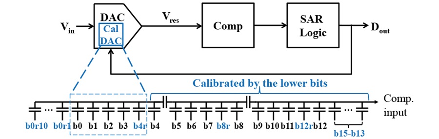

Fig. 16. SAR ADC calibration with existing LSB capacitor array.
The on-chip foreground calibration with minimal overhead proposed here is similar in concept to [17] and [36]. However, we make it possible to calibrate the lower bits as well, which is essential for precision ADCs. The ADC measures the bit weights during calibration and compensates the errors in digital domain during normal operation. Instead of using the back stage or introducing an extra reference DAC to measure the bit weights, some of the LSBs in the ADC (b4r-b0 in this design) are used to calibrate the more significant bits (b4 and above), illustrated in Fig. 16. b4 is measured first with b4r-b0 using the existing SAR ADC feedback loop, while the ADC input is grounded and all the bits above b4 are not trialed. Specifically, we force b4 to 0 and get the ADC output codes which corresponds to the b4 weight at force 0, plus the ADC offset, and then we force b4 to 1 to get another set of output codes, the generalized formulas are shown below:

To remove the offset, we subtract the two to get:

After b4 is calibrated, then b5 is measured with b4-b0, and so on, as generalized in the following equation:

Multiple measurements are taken for each bit weight to average out the effects of noise. This calibration is made possible as redundancy (e.g., b4r) is available to increase the available range for measuring bit weight errors, shown in Fig. 17, otherwise the LSBs would not be able to measure the bit weight if it is larger than nominal weight. Also, as pointed out in [36] and illustrated in Fig. 18, ADC offset eats into the LSB measurement range. To achieve 16-bit level linearity, lower bits like b4 also need to be calibrated. Offsets in the system can be greater than the calibration range for these lower bits. To solve this issue, we introduce offset cancellation with fixed dither during the calibration. Fig. 6(a) illustrated that we have b11-b0 reused as dither capacitors. During the foreground calibration, we measure the ADC offset and cancel it by apply the appropriate amount of offset using the dither capacitors. Thus the ADC appears offset free during the bit weight calibration, enabling us to calibrate much smaller bit weights than those in [17] and [36], which is essential for achieving precision ADC performance.


Fig. 17. Capacitor measurement with redundancy.


Fig. 18. Capacitor measurement with offset compensation by applying a fixed dither amount.
D. Statistical Residue Measurement


Fig. 19. Statistical residue measurement (SRM) for SAR conversion residue. (a) block diagram. (b) Cumulative distribution function (CDF) to derive residue value based on decision probability P.
As previously mentioned, after LSB repeats, the DAC output or comparator input still contains a small residual error Vres. The finite Vres is due to the conversion noise as well as the quantization error. As reported in [37]-[39], we may take advantage of the noisy comparator to measure the value of Vres and thus improve overall ADC accuracy. Fig. 19 illustrates how Vres measurement works. Assume the comparator has Gaussian noise, whose cumulative distribution function (CDF) is defined as:

Where we denote:

We can derive Vres as:

At the end of the regular trials or LSB repeats, the comparator makes a number of sequential decisions with its input unchanged. Based upon the probability of decision 1, the small comparator input can be estimated with (25) given knowledge of the comparator noise level. A small look up table (LUT) in the digital engine can be used to approximate the solution to this nonlinear (25) and the ADC digital output is compensated accordingly. Compared to those in [38] and [39], the number of comparator decisions in our work can be varied in silicon to demonstrate effectiveness and examine trade-offs with measured data.
This technique is only enabled when the ADC is running slower than 16 MS/s so that we have time left in the conversion phase after all the bit trials, allowing for the comparator to fire a number of times afterwards to estimate its input voltage, i.e., the DAC output residual voltage.


Fig. 20. Chip micrograph.


Fig. 21. ADC power breakdown.


Fig. 22. Typical DC linearity plots. (a) DNL before calibration. (b) DNL after calibration. (c) INL before calibration. (d) INL after calibration.


Fig. 23. Typical AC spectrum after calibration with 100 kHz input.


Fig. 24. AC performance. (a) SFDR/SNDR/SNR versus Fin with Fs = 16 MS/s. (b) SFDR/SNDR/SNR versus Fs with Fin = 100 kHz.


Fig. 25. Measured ADC noise with number of LSB repeats.


Fig. 26. Measured ADC noise with number of SRM decisions.


Fig. 27. SFDR comparison with Nyquist ADCs from ISSCC and VLSI in the past 10 years with SFDR > 85 dB or SNDR > 80 dB.
| This work | Hurrell [1] | Bannon [2] | Maddox [3] | Kramer [12] | Miki [29] | |
| Type | SAR | Pipe SAR | Pipe SAR | SAR | SAR | SAR |
| Resolution [bit} | 16 | 18 | 18 | 16 | 14 | 13 |
| Speed [MS/s] | 16 | 12.5 | 5 | 1 | 35 | 50 |
| Power [mW] | 16.3 | 105 | 30.5 | 6.95 | 54.5 | 4.2 |
| SFDR/SNDR [dB] | 98/78 | 82/80 | 100/99 | 100/81 | 99/75 | 85/71 |
| INL [LSB] | -1.9/2.3 | -2.5/2.5 | -2/2 | -0.8/0.8 | -0.9/0.7 | -1.3/2 |
| Cin [pF] | 1.14 | 25 | NA | 25.6 | 0.2 | 2 |
| VDD [V] | 3.3/1.2 | 5/2.5 | 5/1.8 | 1.2 | 2.5/1.2 | 1.2 |
| Area [mm2] | 0.55 | 4.5 | 5.74 | 4.1 | 0.24 | 0.097 |
| Calibration | On chip | Off chip | Off chip | Off chip | Off chip | On chip |
| FoM_S [dB] | 165 | 157.7 | 177.7 | 159.6 | 159.5 | 166.8 |
| Process | 55nm | 250nm | 180nm | 55nm | 40nm | 90nm |
IV. EXPERIMENTAL RESULTS
The chip is fabricated in a 55-nm CMOS process. Die micrograph is shown in Fig. 20 and it measures 1.1 mm by 0.5 mm. The digital engine which also includes calibration is small thanks to the dense logic. The ADC input interface operates at 3.3 V while all other circuits use 1.2 V. By default, optimal LSB repeats is turned on and SRM is turned off to operate at 16 Msps. Fig. 21 shows the power breakdown where the DAC consumes 11.6 mW which also includes the estimated 2.8 mW from the level shifters. With the dramatically reduced sampling capacitance at 1.14 pF (including flash sampling capacitance) for precision ADCs, particular attention was paid to coupling through sub-fF level parasitics to maintain 16-bit linearity performance. Fig. 22 shows the DC linearity performance both with calibration OFF and ON. Before calibration, we see large INL error up to roughly 250 LSBpp mainly due to the charge sharing error from the reservoir capacitors. After calibration, the INL is -1.9/2.3 LSB. It is limited by sampling distortion because input bootstrapping was avoided to support passive sampling in impulse mode. Fig. 23 shows the spectrum with 100 kHz input signal, and the AC performance is summarized in Fig. 24, where SFDR/SNDR/SNR vs Fin and Fs are shown respectively. For most precision applications, input signal bandwidth is below 100 kHz, where over 97.5-dB SFDR is maintained. The SNR is over 78 dB and the equivalent ADC noise is about 3 LSB, meeting our design target. In Fig. 25, the measured ADC noise versus number of LSB repeats is shown to demonstrate its effectiveness. When operating at a lower frequency, statistical residue measurement (SRM) could be enabled to further improve accuracy. Fig. 26 shows the ADC noise versus number of SRM decisions. We observe that the ADC noise does approach the sampling noise level as number of SRM decisions increases. Note that for both noise plots, the conversion noise is configured higher to dominate the sampling noise to better observe the effect. The plot in Fig. 27 compares the linearity performance of this ADC with recent Nyquist ADCs from ISSCC and VLSI in the past 10 years with SFDR > 85 dB or SNDR > 80 dB [40]. Comparison with recently published medium speed and high resolution SAR ADCs is given in Table 1. [1] and [2] use a pipelined SAR architecture and are roughly 10× larger area with 20× larger input capacitance. In addition, all the other precision ADCs (16-bit+) rely on off-chip calibration and thus have much increased test cost.
V. CONCLUSION
A precision 16-bit SAR ADC that achieves 16 MS/s operation in 55-nm CMOS is presented in this paper. It supports both continuous mode and impulse mode operations. The fast conversion and small area is enabled by the small capacitor array and the signal independent, one reservoir-capacitor per bit-capacitor DAC structure. The minimal overhead on-chip calibration that calibrates down to lower bits helps ensure the ADC achieves 16-bit precision. Optimal LSB repeats and statistical residue measurement further improves the ADC accuracy and efficiency. Compared to traditional precision SAR ADCs, this ADC has 10× smaller area, 20× smaller sampling capacitance, and on-chip calibration to make it well-suited for precision SoC applications. To our knowledge, this work is also the first fast precision SAR ADC in a deep sub-micron CMOS node.
About the Authors
(M’10) received the B.Eng. degree in information science and
electronic engineering from Zhejiang University, Hangzhou, China, in 2002, and the
M.Phil. degree in electronic engineering from The Chinese University of
received the B.S., M.S., and Ph.D degrees in electronics and
electrical engineering from Keio University, Yokohama, Japan in 2008, 2010, 2013,
respectively. From 2013 to 2015, he was a design engineer with Analog
received the B.Eng. degree in electrical engineering from
the University of Edinburgh, Scotland, UK, and the M.Eng. degree in electrical
engineering from the University of Limerick, Republic of Ireland, in 2000 and
was born in New York in 1978. He received the B.A. and B.E. degrees
in electrical engineering from Dartmouth College, Hanover, NH, USA, in 2001.
In 2001, he joined Analog Devices, Wilmington, MA, USA, where he is
received the B.S. degree from University of Science and Technology
of China, Hefei, China, in 2005, and the M.S. degree and Ph.D degree in electrical
engineering from Iowa State University, Ames, Iowa in 2010. In
received the B.S. degree in electrical engineering from the University
of Toledo, in 1985 and the M.S. degree in electrical engineering from Cleveland State
University, Cleveland, Ohio, in 1994. From 1988 to 1996, he
was born in Mumbai, India in 1989. He received the B.E.
degree in electronic engineering from University of Mumbai, India in 2011 and M.S
in Computer Engineering from Arizona State University, US in 2014. He served as
Ron Kapusta is an Analog Devices Fellow and holds the B.S. and M.Eng. degrees from the Massachusetts Institute of Technology. Upon graduating in 2002, he joined Analog Devices, designing data converters and sensor
(M’80) received the B.S. degree from the California Institute
of Technology, Pasadena, California, in 1976 and the M.S. and Ph.D. degrees in
electrical engineering from the Massachusetts Institute of Technology,
Related to this Article
Industry Solutions
Product Categories


