X- and Ku-Band Small Form Factor Radio Design
Many aerospace and defense electronics systems in the satcom, radar, and EW/SIGINT fields have long required access to a portion, or all, of the X and Ku frequency bands. As these applications move to more portable platforms such as unmanned aerial vehicles (UAVs) and handheld radios, it is critical to develop new small form factor, low power radio designs that operate in the X and Ku bands, while still maintaining very high levels of performance. This article outlines a new high frequency IF architecture that drastically reduces the size, weight, power, and cost of both the receiver and transmitter without impacting the system specifications. The resulting platform is also more modular, flexible, and software defined than existing radio designs.
Introduction
In recent years, there has been an ever increasing push to achieve wider bandwidths, higher performance, and lower power in RF systems, all while increasing the frequency range and decreasing the size. This trend has been a driver for technology improvements, which have allowed for greater integration of RF components than has been seen before. There are many drivers pushing this trend.
Satcom systems are seeing desired data rates up to 4 Gbps to support transmitting and receiving terabytes of collected data per day. This requirement is pushing systems to operate in the Ku- and Ka-band due to the fact that wider bandwidths and higher data rates are easier to achieve at these frequencies. This demand means a higher density of channels and a wider bandwidth per channel.
Another area of increasing performance requirements is in EW and signals intelligence. Scan rates for such systems are increasing, driving the need for systems that have a quick tuning PLL and wide bandwidth coverage. The drive toward lower size, weight, and power (SWaP) and more integrated systems stems from the desire to operate handheld devices in the field, as well as increase channel density in large fixed location systems.
The advancement of phased arrays are also enabled by further integration of RF systems in a single chip. As integration pushes transceivers smaller and smaller, it allows each antenna element its own transceiver, which in turn enables the progression from analog beamforming to digital beamforming. Digital beamforming provides the ability to track multiple beams at one time from a single array. Phased array systems have a myriad of applications, whether it is for weather radar, EW applications, or directed communications. In many of these applications, the drive to higher frequencies is inevitable, as the signal environment at lower frequencies becomes more congested.
In this article, these challenges are addressed using a highly integrated architecture based upon the AD9371 transceiver as an IF receiver and transmitter, allowing the removal of an entire IF stage and its associated components. Included is a comparison between traditional systems and this proposed architecture, as well as examples of how this architecture can be implemented through a typical design process. Specifically, the use of an integrated transceiver allows for some advanced frequency planning that is not available in a standard superheterodyne style transceiver.
Overview of Superheterodyne Architecture
The superheterodyne architecture has been the architecture of choice for many years due to the high performance that can be achieved. A superheterodyne receiver architecture typically consists of one or two mixing stages, which are fed into an analog-to-digital converter (ADC). A typical superheterodyne transceiver architecture can be seen in Figure 1.

Figure 1. Traditional X- and Ku-band superheterodyne receive and transmit signal chains.
The first conversion stage upconverters or downconverters the input RF frequencies to an out of band spectrum. The frequency of the first IF (intermediate frequency) depends on the frequency and spur planning, as well as the mixer performance and available filters for the RF front end. The first IF is then translated down to a lower frequency that the ADC can digitize. Although ADCs have been making impressive advances in their ability to process higher bandwidths, their upper limit today is around 2 GHz for optimal performance. At higher input frequencies, there are trade-offs in performance vs. input frequency that must be considered, as well as the fact that higher input rates require higher clock rates, which drive up power.
In addition to the mixers, there are filters, amplifiers, and step attenuators. The filtering is used to reject unwanted out of band (OOB) signals. If unchecked, these signals can create spurious that falls on top of a desired signal, making it difficult or impossible to demodulate. The amplifiers set the noise figure and gain of the system, providing adequate sensitivity to receive small signals, while not providing so much that the ADC over saturates.
One additional thing to note is that this architecture frequently requires surface acoustic wave (SAW) filters to meet tough filtering requirements for antialiasing in the ADC. With SAW filters comes sharp roll-off to meet these requirements. However, significant delay as well as ripple are also introduced.
An example of a superheterodyne receiver frequency plan for X-band is shown in Figure 2. In this receiver, it is desired to receive between 8 GHz and 12 GHz with a 200 MHz bandwidth. The desired spectrum mixes with a tunable local oscillator (LO) to generate an IF at 5.4 GHz. The 5.4 GHz IF then mixes with a 5 GHz LO to produce the final 400 MHz IF. The final IF ranges from 300 MHz to 500 MHz, which is a frequency range where many ADCs can perform well.

Figure 2. Example frequency plan for a X-band receiver.
Receiver Specifications—What Matters
Aside from the well known gain, noise figure, and third-order intercept point specifications, some typical specifications that influence the frequency planning for any receiver architecture include image rejection, IF rejection, self generated spurious, and LO radiation.
- Image spurs—RF outside of the band of interest that mixes with LO to generate tone in IF.
- IF spurs—RF at IF frequency that sneaks through filtering before the mixer and shows up as a tone in the IF.
- LO radiation—RF from the LO leaking out to the input connector of the receiver chain. LO radiation gives a means of being detected, even when in a receive only operation (see Figure 3).

Figure 3. LO radiation leaking back through front end.
-
Self generated spurious—spur at IF that results from mixing of clocks or local oscillators within the receiver.
Image rejection specifications apply to both the first and second mixing stage. In a typical application for X- and Ku-Band, the first mixing stage may be centered around a high IF in the 5 GHz to 10 GHz range. A high IF is desirable here, due to the fact that the image falls at Ftune + 2 × IF, as shown in Figure 4. So the higher the IF, the further away the image band will fall. This image band must be rejected before hitting the first mixer, otherwise out of band energy in this range will show up as spurious in the first IF. This is one of the primary reasons why two mixing stages are typically used. If there were a single mixing stage, with the IF in the hundreds of MHz, the image frequency would be very difficult to reject in the front end of the receiver.

Figure 4. Images mixing into IF.
An image band also exists for the second mixer when converting the first IF down to the second IF. As the second IF is lower in frequency (anywhere from a few hundred MHz up to 2 GHz), the filtering requirements of the first IF filter may vary quite a bit. For a typical application where the second IF is a few hundred MHz, the filtering can be very difficult with a high frequency first IF, requiring large custom filters. This can frequently be the most difficult filter in the system to design, due to the high frequency and typically narrow rejection requirements.
In addition to image rejection, the LO power levels coming back from the mixer to the receive input connector must be filtered aggressively. This ensures that the user cannot be detected due to radiated power. To accomplish that, the LO should be placed well outside of the RF pass band to ensure adequate filtering can be realized.
Introducing the High IF Architecture
The latest offering of integrated transceivers includes the AD9371, a 300 MHz to 6 GHz direct conversion transceiver with two receive and two transmit channels. The receive and transmit bandwidth is adjustable from 8 MHz up to 100 MHz, and can be configured for frequency division duplex (FDD) or time division duplex (TDD) operation. The part is housed in a 12 mm2 package and consumes ~3 W of power in TDD mode, or ~5 W in FDD mode. With the advancement of quadrature error correction (QEC) calibrations, an image rejection of 75 dB to 80 dB is achieved.

Figure 5. AD9371 direct conversion transceiver block diagram.
The advancement of performance of the integrated transceiver ICs has opened up a new possibility. The AD9371 incorporates the second mixer, second IF filtering and amplification, and variable attenuation ADC, as well as digital filtering and decimation of the signal chain. In this architecture, the AD9371, which has a tuning range of 300 MHz to 6 GHz, can be tuned to a frequency between 3 GHz and 6 GHz and receive the first IF directly (see Figure 6). With a gain of 16 dB, NF of 19 dB, and OIP3 of 40 dBm at 5.5 GHz, the AD9371 is ideally specified as an IF receiver.

Figure 6. X- or Ku-band transceiver with AD9371 as IF receiver.
With the use of the integrated transceiver as the IF receiver, there is no longer a concern of the image through the second mixer, as is the case with the superheterodyne receiver. This can greatly reduce the filtering required in the first IF strip. However, there must still be some filtering to account for second-order effects in the transceiver. The first IF strip should now provide filtering at two times the first IF frequency to negate these effects—a much easier task than filtering the second image and second LO away, which can be as close as several hundred MHz. These filtering requirements can typically be addressed with low cost, small off the shelf LTCC filters.
This design also provides a high level of flexibility in the system and can be easily reused for different applications. One way that flexibility is provided is in the IF frequency selection. A general rule of thumb for IF selection is to put it in a range that is 1 GHz to 2 GHz higher than the desired spectrum bandwidth through the front-end filtering. For example, if the designer desires 4 GHz of spectrum bandwidth from 17 GHz to 21 GHz through the front end filter, the IF can be placed at a frequency of 5 GHz (1 GHz above the desired bandwidth of 4 GHz). This allows for realizable filtering in the front end. If only 2 GHz of bandwidth is desired, an IF of 3 GHz could be used. Furthermore, due to the software-definable nature of the AD9371, it is easy to change the IF on the fly for cognitive radio applications, where blocking signals can be avoided as they are detected. The easily adjustable bandwidth of the AD9371 from 8 MHz to 100 MHz further allows for avoiding interference near the signal of interest.
With the high level of integration in the high IF architecture, we end up with a receiver signal chain that takes up about 50% of the space required for an equivalent superheterodyne, while decreasing the power consumption by 30%. In addition, the high IF architecture is a more flexible receiver than the superheterodyne architecture. This architecture is an enabler for low SWaP markets where small size is desired with no loss of performance.
Receiver Frequency Planning with the High IF Architecture
One of the advantages of the high IF architecture is the ability to tune the IF. This can be particularly advantageous when trying to create a frequency plan that avoids any interfering spurs. An interfering spur can result when the received signal mixes with the LO in the mixer and generates an m × n spur that is not the desired tone within the IF band.
The mixer generates output signals and spurs according to the equation m × RF ± n × LO, where m and n are integers. The received signal creates an m × n spur that can fall in the IF band and in certain cases, the desired tone can cause a crossover spur at a particular frequency.
For example, if we observe a system designed to receive 12 GHz to 16 GHz with an IF at 5.1 GHz, as in Figure 7, the m × n image frequencies that cause a spur to show up in band can be found with the following equation:


Figure 7. 12 GHz to 16 GHz receiver and transmitter high IF architecture.
In this equation, RF is the RF frequencies on the input of the mixer, which cause a tone to fall in the IF. Let’s use an example to illustrate. If the receiver is tuned to 13 GHz, that means the LO frequency is at 18.1 GHz (5.1 GHz + 13 GHz). Plugging these values into the previous equation and allowing m and n to range from 0 to 3, we get the following equation for RF:

The results are in the following table:
| m | n | RFsum (GHz) | RFdif (GHz) |
| 1 | 1 | 23.200 | 13.000 |
| 1 | 2 | 41.300 | 31.100 |
| 1 | 3 | 59.400 | 49.200 |
| 2 | 1 | 11.600 | 6.500 |
| 2 | 2 | 20.650 | 15.550 |
| 2 | 3 | 29.700 | 24.600 |
| 3 | 1 | 7.733 | 4.333 |
| 3 | 2 | 13.767 | 10.367 |
| 3 | 3 | 19.800 | 16.400 |
In the table, the first row/fourth column shows the desired 13 GHz signal, which is a result of a 1 × 1 product in the mixer. The fifth column/fourth row and eighth column/third row show potentially problematic in-band frequencies that can show up as spurs in band. For example, a 15.55 GHz signal is within the 12 GHz to 16 GHz desired range. A tone at 15.55 GHz on the input mixes with the LO, to generate a 5.1 GHz tone (18.1 × 2–15.55 × 2 = 5.1 GHz). The other rows (2, 3, 4, 6, 7, and 9) can also pose a problem but due to their being out of band, they can be filtered by the input band-pass filter.
The level of the spur is dependent on several factors. The main factor is the performance of the mixer. Since a mixer is inherently a nonlinear device, there exist many harmonics generated within the part. Depending on how well the diodes inside the mixer are matched and how well the mixer is optimized for spurious performance, the levels on the output will be determined. A mixer spur chart is typically included in the data sheet and can help with determining these levels. An example of a mixer spur chart is shown in Table 2, for the HMC773ALC3B. The chart specifies the dBc level of the spurs relative to the desired 1 × 1 tone.
| n × LO | |||||||
| 0 | 1 | 2 | 3 | 4 | 5 | ||
| m × RF | 0 | — | 14.2 | 35 | 32.1 | 50.3 | 61.4 |
| 1 | –1.9 | — | 17.7 | 31.1 | 32.8 | 61.2 | |
| 2 | 83 | 55.3 | 60 | 59.6 | 6 73.7 | 87.9 | |
| 3 | 82.6 | 86.1 | 68 | 68.5 | 61.9 | 85.9 | |
| 4 | 76 | 86.7 | 82.1 | 77.4 | 74.9 | 75.8 | |
| 5 | 69.3 | 74.7 | 85.3 | 87 | 85.1 | 62 | |
With this spur chart, along with an extension of the analysis that was done in Table 1, we can generate a full picture of what m × n image tones may interfere with our receiver and at what level. A spreadsheet can be generated with an output similar to that shown in Figure 8.
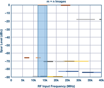
Figure 8. m × n images for 12 GHz to 16 GHz receiver.
In Figure 8, the blue portion shows the desired bandwidth. The lines show different m × n images and their levels. From this chart, it is easy to see what filtering requirements are needed prior to the mixer in order to meet interferer requirements. In this case, there are several image spurs that fall in band and cannot be filtered. We will now look at how the flexibility of the high IF architecture allows us to work around some of these spurs, which is something that the superheterodyne architecture does not afford.
Avoiding Interferers in Receiver Mode
The chart in Figure 9 shows a similar frequency plan that ranges from 8 GHz to 12 GHz, with a default IF at 5.1 GHz. This chart gives a different view of the mixer spurs, showing the center tune frequency vs. m × n image frequency, as opposed to spur level as previously shown. The bolded 1:1 diagonal line in this chart shows the desired 1 × 1 spur. The other lines on the graph represent the m × n images. On the left side of this figure is a representation with no flexibility in the IF tuning. The IF is fixed at 5.1 GHz in this case. With a tune frequency of 10.2 GHz, a 2 × 1 image spur crosses the desired signal. This means that if you are tuned to 10.2 GHz, there is a good chance that a nearby signal could block the reception of the signal of interest. The right plot shows a solution to this problem with flexible IF tuning. In this case, the IF switches from 5.1 GHz to 4.1 GHz near 9.2 GHz. This prevents the crossover spur from occurring.
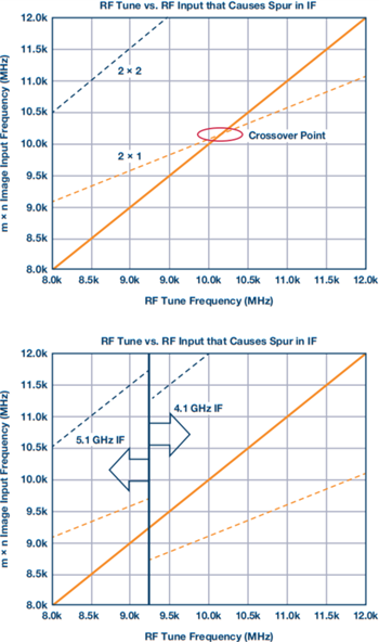
Figure 9. m × n crossover spur with no IF flexibility (top) and avoiding crossover with IF tuning (bottom).
This is just a simple example of how blocking signals can be avoided with the high IF architecture. When coupled with intelligent algorithms to determine interference and calculate new potential IF frequencies, there are many possible ways to make a receiver that can adapt to any spectral environment. It is as simple as determining a suitable IF within a given range (typically 3 GHz to 6 GHz), then recalculating and programming the LO based on that frequency.
Transmitter Frequency Planning with the High IF Architecture
As with the receive frequency planning, it is possible to take advantage of the flexible nature of the high IF architecture to improve spurious performance of the transmitter. Whereas on the receiver side, the frequency content is somewhat unpredictable. On the transmit side, it is easier to predict the spurious on the output of the transmitter. This RF content can be predicted with the following equation:

Where the IF is predefined and determined by the tuning frequency of the AD9371, the LO is determined by the desired output frequency.
A similar mixer chart as was done for the receiver channel can be generated on the transmit side. An example is shown in Figure 10. In this chart, the largest spurs are the image and the LO frequencies, which can be filtered out to desired levels with a band-pass filter after the mixer. In FDD systems where spurious output may desensitize a nearby receiver, in-band spurs can be problematic and this is where the flexibility of the IF tuning can come in handy. In the example from Figure 10, if a static IF of 5.1 GHz is used, there will exist a crossover spur on the output of the transmitter, which will be near 15.2 GHz. By adjusting the IF to 4.3 GHz at a tune frequency of 14 GHz, the crossover spur can be avoided. This is depicted in Figure 11.

Figure 10. Output spurious with no filtering.

Figure 11. Static IF causes crossover spur (top), IF tuning to avoid crossover spur (bottom).
Design Example—Wideband FDD System
To show the performance that can be achieved with this architecture, a prototype receiver and transmitter FDD system was built up with off the shelf Analog Devices components, and configured for 12 GHz to 16 GHz operation in the receive band, and 8 GHz to 12 GHz operation in the transmit band. An IF of 5.1 GHz was used to collect performance data. The LO was set to a range of 17.1 GHz to 21.1 GHz for the receive channel and 13.1 GHz to 17.1 GHz for the transmit channel. The block diagram for the prototype is shown in Figure 12. In this diagram, the X and Ku converter board is shown on the left and the AD9371 evaluation card is shown on the right.

Figure 12. Block diagram for X- and Ku-band receiver and transmitter FDD prototype system.
Gain, noise figure, and IIP3 data was collected on the receive downconverter and is shown in Figure 13 (top). Overall the gain was ~20 dB, NF was ~6 dB, and IIP3 was ~–2 dBm. Some additional gain leveling could be accomplished with the use of an equalizer, or a gain calibration could be performed utilizing the variable attenuator in the AD9371.

Figure 13. Ku-band receiver data (top), X-band transmitter data (bottom).
The transmit upconverter was also measured, recording its gain, 0 P1dB, and OIP3. This data is plotted across frequency in Figure 13 (bottom). The gain is ~27 dB, P1 dB ~22 dBm, and OIP3 ~32 dBm.
When this board is coupled with the integrated transceiver, the overall specifications for receive and transmit are as shown in Table 3.
| Rx, 12 GHz to 16 GHz |
Tx, 8 GHz to 12 GHz |
|||
| Gain | 36 dB | Output Power | 23 dBm |
|
| Noise Figure | 6.8 dB | Noise Floor | –132 dBc/Hz | |
| IIP3 | –3 dBm | OIP3 | 31 dBm | |
| Pin, max (no AGC) | –33 dBm | OP1dB | 22 dBm | |
| In-Band m × n | –60 dBc | In-Band Spurs | –70 dBc | |
| Power | 3.4 W | Power | 4.2 W |
Overall, the performance of the receiver is in line with a superheterodyne architecture, while the power is greatly reduced. An equivalent superheterodyne design would consume more than 5 W for the receiver chain. Additionally, the prototype board was fabricated without a priority to decrease the size. With proper PCB layout techniques, as well integrating the AD9371 onto the same PCB as the downconverter, the overall size of a solution using this architecture could be condensed to just 4 to 6 square inches. This shows significant size savings over an equivalent superheterodyne solution, which would be closer to 8 to 10 square inches. Furthermore, size could be reduced further using advanced packaging techniques such as with a multichip module (MCM) or system in package (SiP) techniques. With these advanced techniques, size could be reduced down to 2 to 3 square inches.
Conclusion
In this article, we have shown a viable alternative architecture, the high IF architecture, which can enable a sizeable improvement in SWaP over the traditional approach. An overview of the superheterodyne was given, as well as a description of specifications of importance in receiver design. The high IF architecture was then introduced, along with explanations of the advantages in terms of filtering requirements and level of integration, to reduce overall part count. We have covered the details surrounding how to go about crafting a frequency plan, as well as a description of how the tunable IF can be utilized to avoid interfering signals on the receiver. On the transmit side, where the goal is to reduce output spurious, we have presented a way to avoid in-band spurious, as well as an approach to predicting all of the output spurious products that may exist.
The enabler of this architecture is the leaps and bounds that the integrated direct conversion receiver has made recently. With the advent of the AD9371, higher performance is realizable with the advanced calibrations and high level of integration. This architecture will become particularly important in low SWaP markets in the coming years.


