UL Recognized, IEEE 1394 Single- and Dual-Port FireWire Protective Circuits
Introduction
After extensive safety testing, the MAX5943A single-port and MAX5944 dual-port FireWire current limiter and low-drop ORing switch controllers have been UL Recognized under the Component Recognition Program of Underwriters Laboratories, Inc.® Note that the circuits themselves, not any individual component thereof, have been UL Recognized. To assist designers with implementing these UL Recognized circuits, this application note provides schematics for each circuit. It also provides the bill of materials (BOM) for each of the two circuits, detailing therein the components required for UL Recognition. Any changes to the basic circuit, or changes to the current-carrying components (the sense resistor or MOSFET switches) of the circuits, would necessitate additional UL testing to achieve UL Recognition. However, increasing the Ohmic value of the sense resistor to decrease the current-limit value is not expected to require additional safety testing.
Neither of these circuits requires a series fuse to achieve the UL's safety specifications, which require safe operation in the event of a single-element failure (open or short circuit) between any two of the three MOSFET or BJT terminals. These circuits meet the UL's safety requirements by employing two MOSFETs placed in series such that one of the two MOSFETs is able to sustain a short circuit from source to drain without compromising the safety of the complete circuit. A network of four resistors and two pnp transistors are placed between the MOSFET gates and the controller IC to isolate and drive the two individual MOSFETs from the single gate-control signal (per channel in the two-port circuit) from the controller IC. UL testing was performed with a 12V power source.
Circuit Description
Figure 1 illustrates a single-port FireWire protective circuit implemented with the MAX5943A. Input power of 7.5V to 37V is applied at the input VIN, and a load is connected from pin 1 to pin 2 of the 6-pin IEEE 1394 connector at the output. Load current flowing through sense-resistor R2 generates the current-sense voltage applied from pin 16 to pin 15 of the MAX5943A controller IC. When this sensed voltage reaches a 50mV ±5% threshold level, the output current is regulated to maintain a constant sensed voltage. If the regulated current continues beyond 2ms, the controller automatically disconnects the load, although the current can continue indefinitely at any value below the 50mV threshold.
Under steady-state conditions, GATE2 is driven ≈5.5V higher than VIN to enhance MOSFET N2. When output current reaches the limiting value, the voltage at GATE2 drops to maintain current at the set point until the current-limit timeout occurs, or until the output current drops below the set point. Upon load disconnect, the GATE2 voltage drops quickly to zero, the fault signal is set, and the controller waits for 256ms before attempting a restart. If an overload still exists, the timeout and automatic restart will continue indefinitely, setting the current-limited duty cycle to < 0.8%. The circuit, therefore, operates safely under continuous short-circuit conditions.
The circuit provides:
- 2.5A (adjustable) current limiting to the load at initial connection or during an overcurrent fault condition
- 2ms (adjustable) current-limit timeout before load disconnect for excessive load current
- Automatic-restart attempts after a fault shutdown condition
- < 0.8% current-limited duty cycle during continuous fault condition
- 6.5V undervoltage shutdown protection
- Low-drop ORing in multiple-power-source applications
- Fault reporting
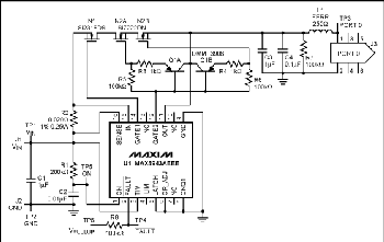
MOSFET N1 is the ORing device that allows the output to be supplied by more than one supply circuit. The ORing function protects the system's power supply from being backfed from a power-providing peripheral when that peripheral's power-source voltage exceeds the system power-source voltage. At very low load currents, N1 is off, and load current flows unidirectionally through its body diode. When the sense voltage drop across sense-resistor R2 reaches 5mV (load current = 0.25A), N1 is turned on to provide a low-drop ORing function. If the alternate supply-circuit voltage exceeds VIN - VF (N1BODY DIODE), no current flows from VIN.
In a fused circuit, Q1, R3, R4, R5, and R6 are unnecessary and switch N2 need only be a single MOSFET. In this fuseless circuit, placing MOSFETs N2A and N2B in series allows for a single-element failure in either N2A or N2B without loss of short-circuit load disconnect.¹ Q1 and the four resistors isolate the two MOSFET gates from one another, even though they are driven from the single GATE2 output of U1. R5 and R6 allow gate isolation when GATE2 is driven high to turn on the MOSFETs. R3, R4, and Q1 allow gate isolation when GATE2 is driven low; yet, they also allow rapid discharge of MOSFET gate capacitances for quick turn off.
Optional connections at U1 terminals 3, 4, 5, 6, and 8 allow modified operation from the conditions chosen. Connections at TIM allow a 220µs to 175ms current-limit timeout period. Connections at ILIM allow one to adjust the circuit-breaker threshold to 40, 50, or 60mV. Connections at LATCH allow either latching or autorestart fault management. Connections at OR_ADJ allow an ORing switch turn-on threshold of 5, 7.5, or 10mV. And connections at ONQ1 allow one to disable the ORing function. Refer to the MAX5943A data sheet for connection details. VPULLUP must be connected either to VIN or to another power source in order to read the active-low FAULT signal.
Several minor circuit details are:
- Capacitor C1 may not be required in a permanently operating circuit, but it is included in the test board to damp any input-voltage ringing that might result from quick load disconnect due to inductive power-supply leads that may be present in a board-test configuration. With some power sources, or if power-source connecting leads are long, a larger input capacitor should be mounted outboard of the described test board.
- Capacitor C4 is present at the output to protect U1 by damping any output-voltage ringing due to load disconnect when N2 is turned off by controller U1.
- Resistor R7 is present to discharge C3 and C4 when N2 is turned off for any reason.
- Inductor L1 and capacitor C4 are present to isolate the protective circuit from high-frequency noise on the output line; the impedance of L2 is 250Ω measured at 100MHz.
- R2-C2 constitutes an R-C filter from VIN to the ON terminal of U1. This terminal can be driven low to turn-off the controller. A resistor can be placed across C2 to set the undervoltage lockout (UVLO) to greater than the default value of ≈6.5V. The ON threshold at pin 1 is 1.24V.
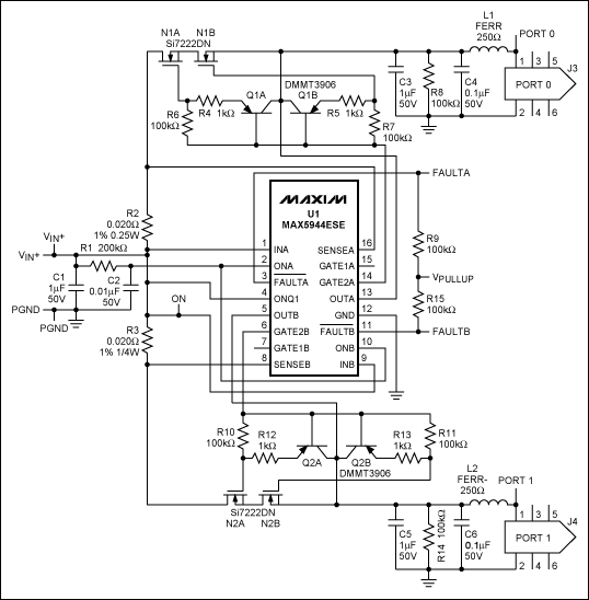
Figure 2 illustrates a dual-port FireWire protective circuit. Its operation is much the same as the circuit in Figure 1 except that no ORing MOSFETs are included. ORing functions can be provided by adding ORing MOSFETs ahead of N1 and N2, connecting GATE1A and GATE1B to the respective ORing MOSFET gates, and grounding pin 4 (ONQ1), instead of connecting it to VIN. Protective features against single-element failures are identical in each channel to those of the single-port protective circuit.
The MAX5943A and MAX5944 operate with input voltages from 7.5V to 37V to meet FireWire specifications. The UVLO voltage is ≈6.5V. The external MOSFETs remain off as long as VIN < 6.5V and VON < 1.24V. To reject transient signals at VIN, VON is connected to VIN through an R-C time delay at R1/C2. If a UVLO > 6.5V is desired, a resistor can be placed across C2 to create the desired turn-on voltage. The VON threshold is 1.24V.
UL Recognition
UL Recognition is extended to these circuits with either the MAX5943A or MAX5944, the specific make and model of N1 and N2, the specific make and model of the 0.02Ω 0.25W sense resistor, the equivalent copper-pad heatsink area for the pass MOSFETs, and the default current-limit timing set at 2ms by the connection of TIM to VIN. With a current-limit sense voltage of 50mV and a sense-resistor value of 0.02Ω, the current-limit setting is 2.5A. A lower current-limit value could fall within UL Recognition criteria but not a higher current-limit value. Equivalent sense-resistor and MOSFET characteristics may be allowed under UL practices, but no assurances can be given that any circuit or component changes are acceptable if UL Recognition is to be retained. UL testing was performed with a 12V input-source voltage.
The current-limit timeout is set at 2ms by default with TIM connected to VIN. This is the condition under which UL Recognition has been obtained. During startup, a large capacitor at C3 may result in a charging current equivalent to the current limit. With a large C3, the charging time could exceed the 2ms current-limit timeout, causing the MAX5943A/MAX5944 to shutdown. A large C3 could be accommodated by increasing the current-limit timeout beyond the default 2ms. However, UL Recognition of this system depends upon safe power-dissipation limits in the pass MOSFET, and a longer current-limit timeout could result in higher peak junction temperature in the MOSFET under short-circuit conditions. Thus, UL Recognition could be adversely affected if the current-limit timeout is set greater than the default value of 2ms.
The dual-port system is specifically designated by UL as "Low-Voltage Solid-State Overcurrent Protector, Type MAX5944—For Use In System Firewire Protective Circuit, Version 1."
The single-port system is specifically designated by UL as "Low-Voltage Solid-State Overcurrent Protector, Type MAX5943A—For Use In System Firewire Protective Circuit, Version 2."
PCB Layout
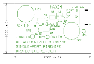
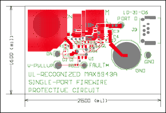
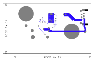
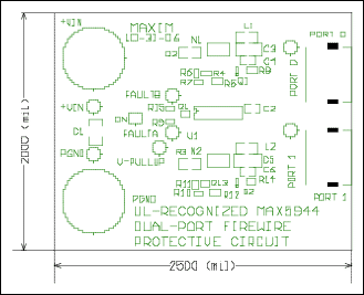
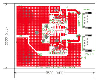
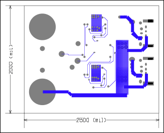
The PCB layout for the single-port FireWire protective circuit is detailed in Figures 3, 4, and 5. The PCB layout for the dual-port FireWire protective circuit is detailed in Figures 6, 7, and 8. Note that in both cases significant copper heatsink area is associated with the sense resistors and with each power MOSFET. Layout details are not part of UL Recognition, although sufficient MOSFET copper heatsink area should be provided in any re-creation of these circuits as needed to limit peak MOSFET junction temperature to safe limits under maximum-load or short-circuit conditions. For thermal calculations, see the transient thermal characteristics of each MOSFET.
Summary
This application note describes UL Recognized FireWire protective circuits for a single-port system (MAX5943A) and a dual-port system (MAX5944). To assist designers with implementing these circuits, this application note details the schematics, method of operation, component specifications, and PCB layout for each circuit. System limitations to UL Recognition are also described and discussed. It is noted that UL Recognition has been obtained for the circuits themselves, not any individual component thereof. Consequently, any changes to the basic circuits or their current-carrying components would necessitate additional UL testing to achieve UL Recognition.
| Designation | Quantity | Description | Manufacturer and Part No. |
| C1, C3 | 2 | Ceramic capacitor 1µF 20% 50V X7R 1206 | TDK C3216X7R1H105K |
| C2 | 1 | Ceramic capacitor 10nF 10% 50V X7R 0603 | TDK C1608X7R1H103K |
| C4 | 1 | Ceramic capacitor 100nF 10% 50V X7R 0603 | TDK C1608X7R1H104K |
| J3 | 1 | Connector female IEEE 1394 PC-mount right-angle | Assmann Electronic Components A-IE-S-DIP-R, Astron Technology Corp. 21-0103-6-1T, Cypress Industries 85-32007-101 |
| L1 | 1 | Inductor SMT 250Ω at 1MHz, 2.8A, 50mΩ 0805 | Ceratech HH-1T2012-251, World Products WPBH-T2012-251T |
| N1 | 1 | MOSFET N-channel 58mΩ, 3.9A, 40V SOT23 | Vishay Si2318DS |
| Q1 | 1 | Transistor bipolar pnp dual SOT23-6 | DMMT3906W |
| R1 | 1 | Resistor SMT 200kΩ 0402 | |
| R2 | 1 | Resistor SMT 0.02Ω 1% 0.25W 0805 | Cyntec RL1220T-R020-FN |
| R3, R4 | 2 | Resistor SMT 1kΩ 0402 | |
| R5, R6, R7, R8 | 4 | Resistor SMT 100kΩ 0402 | |
| U1 | 1 | IC controller hot-swap ORing QSOP-16 | Maxim MAX5943AEEE |
| Designation | Quantity | Description | Manufacturer and Part No. |
| C1, C3, C5 | 3 | Ceramic capacitor 1µF 20% 50V X7R 1206 | TDK C3216X7R1H105K |
| C2 | 1 | Ceramic capacitor 10nF 10% 50V X7R 0603 | TDK C1608X7R1H103K |
| C4, C6 | 2 | Ceramic capacitor 100nF 10% 50V X7R 0603 | TDK C1608X7R1H104K |
| J1, J2 | 2 | Connector female banana uninsulated | |
| J3, J4 | 2 | Connector female IEEE 1394 PC-mount right-angle | Assmann Electronic Components A-IE-S-DIP-R, Astron Technology Corp 21-0103-6-1T, Cypress Industries 85-32007-101 |
| L1, L2 | 2 | Inductor SMT 250Ω at 1MHz, 2.8A, 50mΩ 0805 | Ceratech HH-1T2012-251, World Products WPBH-T2012-251T |
| N1, N2 | 2 | MOSFET N-channel dual 47mΩ, 6A, 40V 1212-8 Pwr Pkg | Vishay Si7222DN |
| Q1, Q2 | 2 | Transistor bipolar pnp dual SOT23-6 | DMMT3906W |
| R1 | 1 | Resistor SMT 200kΩ 0402 | |
| R4, R5, R12, R13 | 5 | Resistor SMT 1kΩ 0402 | |
| R6, R7, R8, R9, R10, R11, R14, R15 | 8 | Resistor SMT 100kΩ 0402 | |
| U1 | 1 | IC controller hot-swap ORing dual SO-16 | Maxim MAX5944ESE |
Appendix
Effect Analysis of Single-Element Failures in N2A, N2B, Q1A, and Q1B (Ref. Figure 1)
The circuit in Figure 1 was evaluated to determine the effects of single-element failures and, ultimately, to justify eliminating the fuse as a safety element to protect against an output short circuit.
This circuit should be able to support a single-element failure on Q1A, Q1B, N2A, or N2B without causing a serious overcurrent condition in the event of an output short circuit. The failure mode considered is a short circuit between any two of the three terminals of N2A, N2B, Q1A, or Q1B.
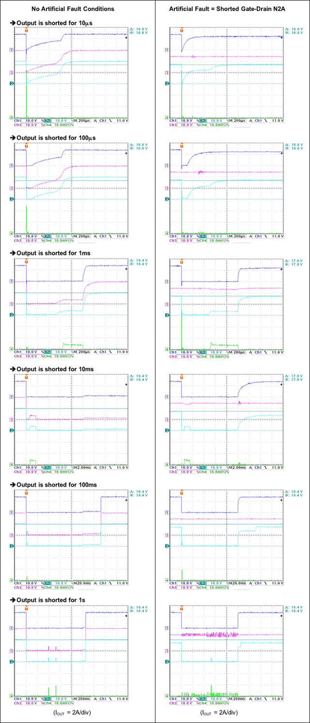
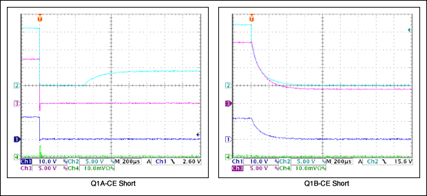
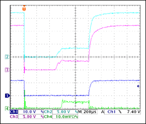
The set of reference waveforms provided in this appendix show: CH1 = VOUT, CH2 = N2BGATE, CH3 = N2AGATE, and CH4 = IOUT (5A/div) when an output short circuit is applied with no simulated shorts applied to N2A, N2B, Q1A, or Q1B.
All succeeding waveforms contain the same four traces as labeled here. The output short-circuit test lasts for 1ms. The input voltage is 12V. There is a 100Ω = 120mA load other than the test short circuit. Initially, the fast comparator senses an overcurrent condition and shuts down both gates.
About 0.5ms later, both gates rise and stabilize at a VGS that supports the programmed limiting current of 2.5A.
When the short circuit is removed at 1ms, all waveforms return to their normal levels.
If the short circuit continues beyond 1ms, the device shuts down after the programmed 2ms overcurrent timeout period. Then, a delayed restart occurs 256ms later. This continues until the short circuit is removed.
- A Q1A or Q1B base-emitter short merely bypasses the 100kΩ series gate resistor with a 1kΩ resistor, causing no failure.
A Q1A or Q1B collector-emitter short places a 1kΩ resistor between the corresponding gate and the output. No load current passes from input to output; hence, the circuit is safe, although inoperative. Although the output will rise eventually (≈0.5µs) when there is no load, the output will not rise with any reasonable connected-load resistance. Alternately, if the output has risen with no load, the output drops out completely when any load is connected. The corresponding gate drive is ≈0V, while the GATE2 terminal and the alternate gate rises to ≈4V above GND due to the pullup current of ≈40µA flowing through the 100kΩ + 1kΩ resistors now series-connected from GATE2 to GND through the load resistor.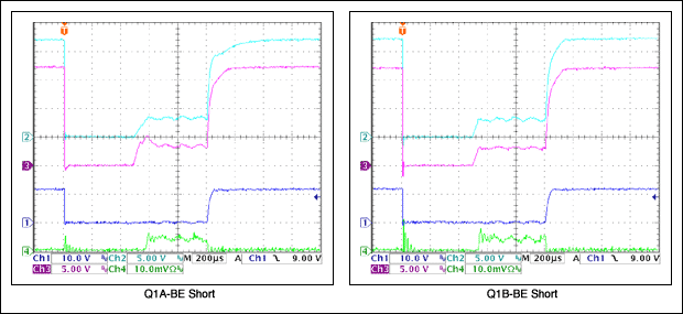
Figure 9B. Waveforms showing the effects of a Q1A or Q1B base-emitter short. Operation is shown to be similar to that of the reference waveform with no unusual behavior.
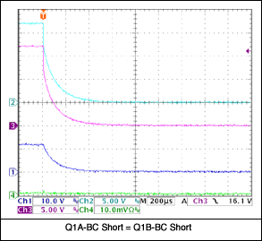
- A Q1A or Q1B base-collector short creates a short from GATE2 to the output—therefore, neither FET will turn-on. If the circuit was previously on, the circuit has safely shutdown.
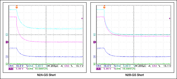
- An N2A or N2B gate-source short turns off the corresponding FET to safely shutdown the circuit. The operation is similar to that of the Q1A or Q1B collector-emitter short described in #2 above, except that the alternate FET is on because its gate rises ≈4V above the input voltage.
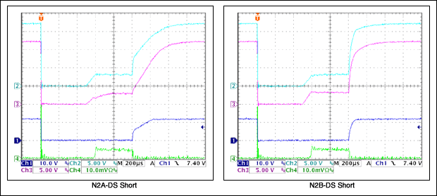
- An N2A or N2B gate-drain short causes the shorted device to operate at VGS ≈ VGS(TH), causing device overheating and, eventually, a device short-circuit drain-source-gate in the presence of a prolonged output short circuit.
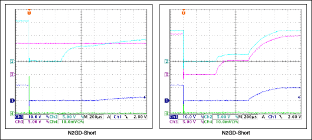
When N2-GD is shorted, N2 gate voltage = the input voltage. This causes the N2 source voltage to be the value of VGS(TH) below the gate voltage. The N2 drain-source resistance is approximately 10Ω.
If N2 sustains a gate-drain short that eventually causes N2 to short between all pins, the circuit operates as follows. (Calculations are for VIN = 12V.)
- Condition 1: GATE2 = high with 45µA (typ) gate pullup current. Attempted high would be VIN + 5.5V, but the full 45µA would be dissipated in the 100kΩ series gate resistor, thus lowering the actual VGS(ON) to 45µA x 100kΩ = 4.5V.
- Condition 2: GATE2 in fast pull-down mode due to an output short circuit. Attempted pull-down current > 125mA (possibly as high as 1A). Conditions are:
- VOUT ≈ 0V
- GATE2 (pin 12) sinking up to 125mA current to GND from the base of Q1A and Q1B
- Q1A and Q1B base ≈ 0V
- Q1A emitter ≈ 0.6V, 11.4mA flowing through the 1kΩ resistor connecting the N2A gate to the Q1A emitter
- Q1B emitter < 0.6V, fast pull-down of the N2B gate via Q1B to VOUT ≈ 0V
- N2B turns off quickly
Additional information:
VIN = 14V, CH1 = VOUT, Ch2 = VGN2B, CH3 = VGN2A, CH4 = IOUT (5A/div unless noted)
