Triple 300MHz Current Feedback Amplifiers Drive RGB/Component Video and LCD Displays
Triple 300MHz Current Feedback Amplifiers Drive RGB/Component Video and LCD Displays
Sep 1 1999
Introduction
With the advent of HDTV and DVD video, there is a renewed focus on RGB/component video to maximize picture quality. LCD displays have also entered the mainstream for high end and portable computer displays. Both of these applications require high speed triple amplifiers for routing and conditioning video signals. LCD displays also require voltage swings of over 10V, with fast settling, into large capacitive loads. With these applications in mind, Analog Devices has introduced the LT1399 and LT1399HV triple current feedback amplifiers. The LT1399 and LT1399HV contain three independent 300MHz current feedback amplifiers, each with a shutdown pin. Each amplifier has exceptional 0.1dB gain flatness of 150MHz and a slew rate of 800V/µs. Output drive current is a minimum of 80mA over temperature.
The LT1399 operates on all supplies from a single 4V to ±6V. The LT1399HV supports higher supply voltages and will operate on supplies ranging from a single 4V to ±7.5V. Each of the three amplifiers draws 4.6mA when active. When disabled, each amplifier draws zero supply current and its output becomes high impedance. Each amplifier can be enabled in 30ns and disabled in 40ns, making the LT1399 and LT1399HV ideal in spread-spectrum and portable equipment applications.
With the addition of a small series resistor at the output, the LT1399 and LT1399HV are capable of driving large capacitive loads. The LT1399HV’s high voltage operation, when combined with its ability to drive capacitive loads, makes it ideal for driving LCD displays.
What’s Inside
Figure 1 is a simplified schematic for one of the three amplifiers found in the LT1399/LT1399HV. Tying EN low allows current to flow through J1, Q1–Q4 and R1. Q3 and Q6 mirror this current on top, while Q5 and Q7 mirror the current on the bottom. Q6 and Q7 thus act as current sources for input-stage transistors Q8–Q11. +IN is a high-impedance input, driving the bases of Q8 and Q9. The emitters of these transistors then drive the bases of Q10 and Q11, which have their emitters tied together and form a buffered representation of +IN. This node is the inverting input –IN. Any current flowing into or out of –IN modulates the collector currents of Q12 and Q14. This, in turn, modulates the collector currents of Q13 and Q15, which drive the high impedance node. Transistors Q16–Q21 and resistors R2 and R3 form the output stage that buffers the signal at the high impedance node from the output.
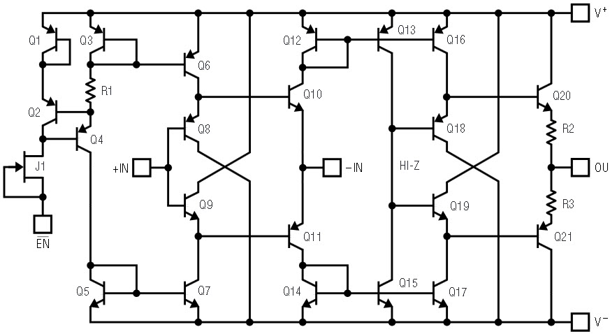
Figure 1. LT1399 simplified schematic (one amplifier).
Using the LT1399HV to Drive LCD Displays
Driving present-day XGA and UXGA LCD displays can be a difficult problem because they require drive voltages of up to 12V, usually present a capacitive load of over 300pF and require fast settling. The LT1399HV is particularly well suited for driving these LCD displays because it is capable of swinging more than ±6V on ±7.5V supplies and, with a small series resistor RS at the output, can drive large capacitive loads with good settling time. This circuit topology can be seen in Figure 2. As seen in Figure 3, at a gain of three, with a 16.9Ω output series resistor and a 330pF load, the LT1399HV is capable of settling to 0.1% in 30ns for a 6V step. Similarly, as seen in Figure 4, a 12V output step will settle in 70ns.
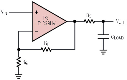
Figure 2. Adding an output series resistor for driving capacitive loads.
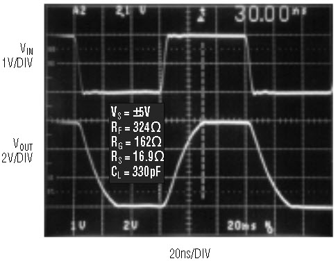
Figure 3. LT1399/LT1399HV large-signal pulse response driving 330pF (typical LCD loading).
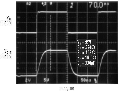
Figure 4. LT1399HV output-voltage swing is >12V with ±7V supplies.
A 3-Input Video Multiplexer and Cable Driver
Figure 5 shows a low cost, 3-input video MUX cable driver. The scope photo in Figure 6 displays the cable output of a 30MHz square wave driving 150Ω. In this circuit, the active amplifier is loaded by the sum of RF and RG of each disabled amplifier. Resistor values have been chosen to keep the total back termination at 75Ω while maintaining a gain of one at the 75Ω load. Figure 7 shows the envelope of the output signal as the multiplexer is switched from channel A to channel B. Channel A is being driven by a 2VP-P, 3.58MHz sine wave. The switching envelope of the output is well behaved and the switching time is approximately 32ns.
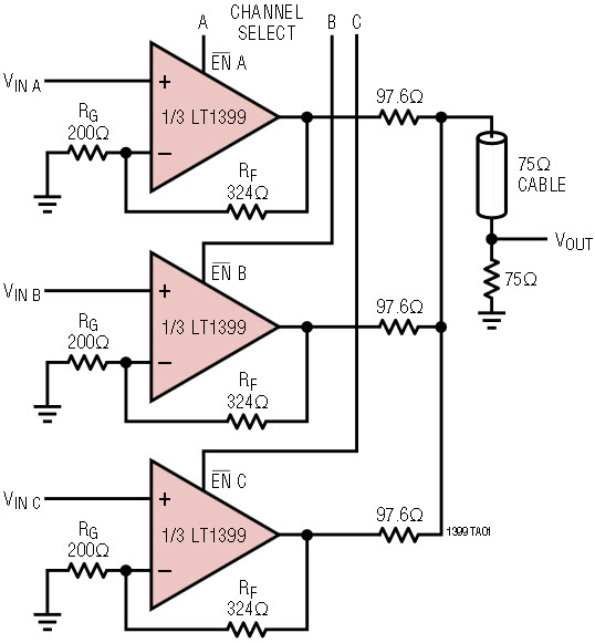
Figure 5. 3-input video mux/cable driver.
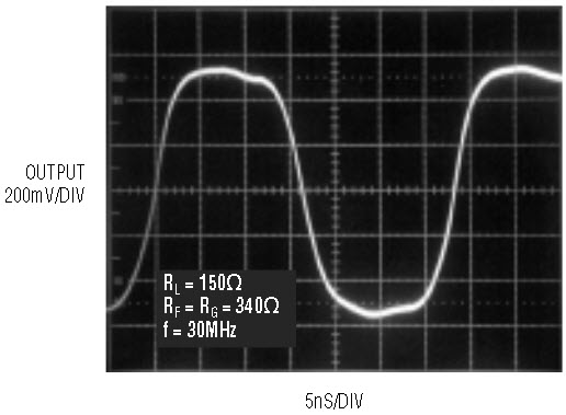
Figure 6. 30MHz square wave response.
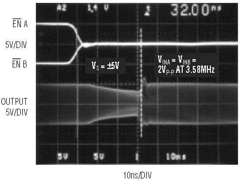
Figure 7. 3-input video mux switching response.
Buffered RGB to Color-Difference Matrix
Two LT1399s can be used to create buffered color-difference signals from RGB inputs. In the application shown in Figure 8, a total of four amplifiers is used to create color-difference signals. The luminance signal Y is created using amplifiers A2 and A3. The remaining color-difference signals each use a single amplifier and the newly created Y output to perform the appropriate difference function.
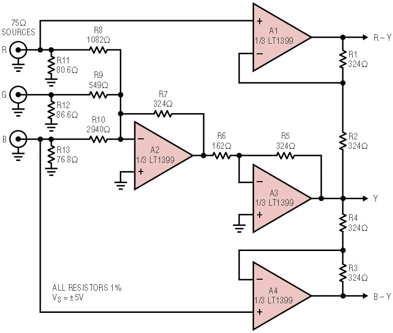
Figure 8. Buffered RGB to color-difference matrix.
The R input arrives via 75Ω coax and is routed to 1082Ω resistor R8 and the noninverting input of LT1399 amplifier A1. There is also an 80.6Ω termination resistor, R11, which yields a 75Ω input impedance at the R input when considered in parallel with R8. R8 connects to the inverting input of a second amplifier, A2, which also sums the weighted G and B inputs to create a –0.5 • Y output. Amplifier A3 then takes the –0.5 • Y output and amplifies it by a gain of minus two, resulting in the Y output. Amplifier A1 is configured in a noninverting gain-of-two configuration, with the bottom of the gain resistor R2 tied to the Y output. The output of amplifier A1 thus results in the color-difference output R – Y.
The B input is similar to the R input. It arrives via 75Ω coax and is routed to 2940Ω resistor R10 and the noninverting input of amplifier A4. There is also a 76.8Ω termination resistor R13, which yields a 75Ω input impedance when considered in parallel with R10. R10 also connects to the inverting input of amplifier A2, adding the B contribution to the Y signal as discussed above. Amplifier A4 is configured in a noninverting gain-of-two configuration with the bottom of the gain resistor R4 tied to the Y output. The output of amplifier A4 thus results in the color-difference output B – Y.
The G input also arrives via 75Ω coax and adds its contribution to the Y signal via a 549Ω resistor R9 that is tied to the inverting input of amplifier A2. There is also an 86.6Ω termination resistor, R12, which yields a 75Ω termination when considered in parallel with R9. Using superposition, it is straightforward to determine the output of amplifier A2. Although inverted, it sums the R, G and B signals in the standard proportions of 0.3R, 0.59G and 0.11B, which are used to create the Y signal. Amplifier A3 then inverts and amplifies the signal by two, resulting in the Y output. Two additional LT1399 amplifiers remain unused, available for additional signal conditioning as needed.
Buffered Color-Difference to RGB Matrix
The LT1399 can also be used to create buffered RGB outputs from color-difference signals. As seen in Figure 9, the R output is a back-terminated 75Ω signal created using resistor R5 and LT1399 amplifier A1 configured for a gain of two via 324Ω resistors R3 and R4. The noninverting input of amplifier A1 is connected via 1k resistors R1 and R2 to the Y and R – Y inputs, respectively, resulting in cancellation of the Y signal at the amplifier input. The remaining R signal is then amplified by A1.
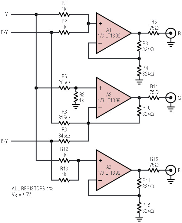
Figure 9. Buffered color-difference to RGB matrix.
The B output is also a back-terminated 75Ω signal created using resistor R16 and amplifier A3 configured for a gain of two via 324Ω resistors R14 and R15. The noninverting input of amplifier A3 is connected via 1kΩ resistors R12 and R13 to the Y and B – Y inputs respectively, resulting in cancellation of the Y signal at the amplifier input. The remaining B signal is then amplified by A3.
The G output is the most complicated of the three. It is a weighted sum of the Y, R – Y and B – Y inputs. The Y input is attenuated via resistors R6 and R7 such that amplifier A2’s noninverting input sees 0.83Y. Using superposition, we can calculate the positive gain of A2 by assuming that R8 and R9 are grounded. This results in a gain of 2.41 and a contribution at the output of A2 of 2Y. The R – Y input is amplified by A2 and resistors R8 and R10, giving a gain of –1.02. This results in a contribution at the output of A2 of 1.02Y – 1.02R. The B – Y input is amplified by A2 and resistors R9 and R10, giving a gain of –0.37. This results in a contribution at the output of A2 of 0.37Y – 0.37B.
If we now sum the three contributions at the output of A2, we get:

It is important to remember though, that Y is a weighted sum of R, G, and B such that:

If we substitute for Y at the output of A2, we then get:

The back-termination resistor R16 then halves the output of A2, resulting in the G output.
Single-Supply RGB Video Amplifier
The LT1399 can be used with a single supply voltage of 6V or more to drive ground-referenced RGB video. As seen in Figure 10, two 1N4148 diodes, D1 and D2, have been placed in series with the output of the amplifier A1, but within the feedback loop formed by resistor R8. These diodes effectively level-shift A1’s output downward by 2 diodes, allowing the circuit output to swing to ground.
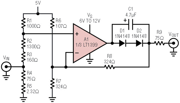
Figure 10. Single-supply RGB video amplifier (one of three channels).
Amplifier A1 is used in a positive gain configuration. The feedback resistor R8 is 324Ω. The gain resistor is created from the parallel combination of R6 and R7, giving a Thevenin-equivalent 80.4Ω connected to 3.75V. This gives an AC gain of five from the noninverting input of amplifier A1 to the cathode of D2. However, the video input is also attenuated before arriving at A1’s positive input. Assuming a 75Ω source impedance for the signal driving VIN, the Thevenin-equivalent signal arriving at A1’s positive input is 3V + (0.4 • VIN), with a source impedance of 714Ω. The combination of these two inputs gives an output at the cathode of D2 of 2 • VIN with no additional DC offset. The 75Ω back termination resistor R9 halves the signal again such that VOUT equals a buffered version of VIN.
It is important to note that the 4.7µF capacitor C1 is required to maintain the voltage drop across diodes D1 and D2 when the circuit output drops low enough that the diodes might otherwise be reverse biased. This means that this circuit works fine for continuous video input, but will require that C1 be charged after a period of inactivity at the input.
Conclusion
Analog Devices has introduced the LT1399 and LT1399HV triple 300MHz current feedback amplifiers. Both of these products are well suited for use in component video applications. The higher supply voltage rating of the LT1399HV makes it an excellent choice for LCD driver applications. Both products feature 4.6mA of supply current per amplifier, 300MHz –3dB bandwidth, an exceptional 0.1dB gain flatness of 150MHz, 800V/µs slew rate and a shutdown pin for each channel.


