The MAX2361 for (1750MHz) Korean Band PCS-CDMA Transmitter Application
Abstract
This application note describes an application of the MAX2361 quadrature transmitter IC in the Korean PCS band (Tx = 1750MHz–1780MHz). From I/Q base-band inputs to the RF pre-driver output, a complete integrated transmit solution is presented that achieves better than -55dBc adjacent channel power ratio (ACPR) with +10dBm of output power.
Additional Information
Introduction
This application note describes an application of the MAX2361 quadrature transmitter IC in the Korean PCS band (Tx = 1750MHz–1780MHz). From I/Q base-band inputs to the RF pre-driver output, a complete integrated transmit solution is presented that achieves better than -55dBc adjacent channel power ratio (ACPR) with +10dBm of output power.
General Description
The MAX2361, along with all products in the MAX236X family, is a complete quadrature transmitter. Included on-chip are a quadrature modulator, variable-gain intermediate frequency (IF) and radio frequency (RF) amplifiers, an image rejecting upconvert mixer, and dual RF and IF synthesizers.
The MAX2361 transmitter is designed to work for dual-band operation and supports AMPS for the cellular band, code division multiple access (CDMA) for the PCS and cellular bands, and wideband code division multiple access (W-CDMA). The desired mode of operation is programmed using a 3-wire serial bus. The MAX2361 includes two IF voltage controlled oscillators (VCOs), two IF input and output ports, two RF local oscillator (LO) input ports, and three power amplifier (PA) driver ports, eliminating off-chip band-switching hardware.
Test Setup
Tests were conducted using an engineering development board and the setup is shown in Figure 1. All data were recorded under the following conditions at room temperature:
VBAT = 3.6VDC (for PA driver bias)
VCC = 2.8VDC (to MAX2361)
External RF LO = -9dBm single-ended at LOH
Baseband input = 400mVP-P Differential, see Figure 2.
I.F. Freq. = 130.38MHz
RF Freq. = 1750MHz to 1780MHz
Reference Freq. = 19.2MHz
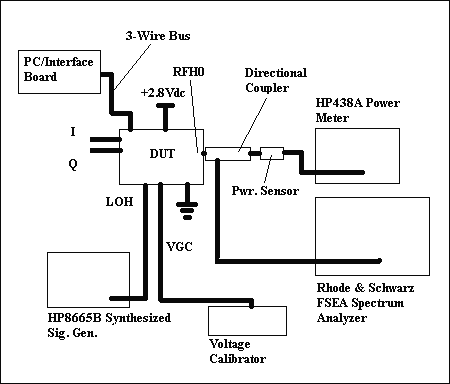
Figure 1. Test setup diagram.
The in-phase and quadrature (I/Q) baseband signals were derived from an Agilent 4433B signal generator set to deliver an IS-95A reverse CDMA channel. External resistor dividers were used to decrease the I/Q signal amplitude to approximately 400mVP-P differential (200mVP-P single ended), see Figure 2.

Figure 2. Single ended in-phase/quadrature signal (measured at MAX2361 input).
The baseband signals were then applied to the MAX2361 I/Q inputs, up-converted, and amplified to a 130.38MHz IF by the quadrature modulator and IF variable gain amplifier (VGA). The IF was routed off-chip through a lumped element LC filter, and back on-chip to be further up-converted to RF by an image-reject mixer and RF VGA. The output driver match was accomplished using a single pull-up inductor and a series capacitor.
The IF LO signal was generated and regulated by the on-chip synthesizer in conjunction with external tank and loop filter components comprising an IF phase-locked loop (PLL). Also external was the 19.2MHz temperature compensated crystal oscillator which provides the PLL reference frequency.
Although an external RF VCO module, loop filter, and internal RF PLL synthesizer could have been used the requisite VCO module was not available at the time of testing. The RF LO was thus provided by an external signal generator set to deliver the appropriate high-side injection signal at approximately -9dBm.
The mode of operation, IF PLL dividers, and IF VGA gain were set via the 3-wire bus interface software (see Figure 3) while an external voltage calibrator was used to simulate a digital to analog converter (DAC) voltage at the VGC pin. Power and linearity measurements were taken simultaneously through the use of a directional coupler.
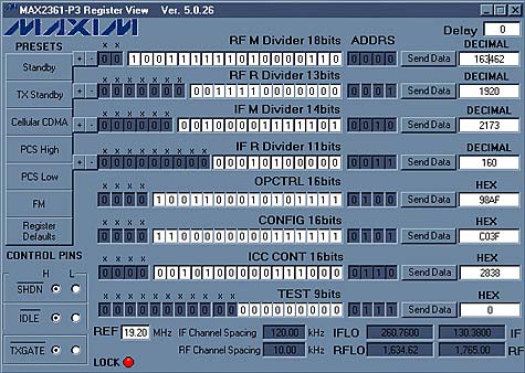
Figure 3. Interface software settings.
For a schematic diagram of the MAX2361 Korean Band test circuit see Figure 4.

Figure 4.
Table 1 presents the actual lab recorded data. For each frequency (1750MHz, 1765MHz, and 1780MHz) the gain control voltage is varied through its range and the ACPR, output power and supply current are recorded.
| VGC (V) |
I.F. Gain Setting* |
POUT (dBm) |
ACP1 (dBc) |
ALT1 (dBc) |
Icc (mA) MAX2361 |
|
| 1750MHz | 2.40 | 100 | 9.83 | -56.1 | -72.3 | 128 |
| 2.38 | 100 | 8.64 | -56.4 | -72.3 | 118 | |
| 2.36 | 100 | 6.86 | -55.9 | -72.2 | 106 | |
| 2.34 | 100 | 5.27 | -54.6 | -72.4 | 96 | |
| 2.32 | 011 | 0.92 | -58.1 | -72.5 | 87 | |
| 2.30 | 011 | -0.78 | -57.2 | -71.5 | 8 | |
| 2.28 | 011 | -2.80 | -56.8 | -72.2 | 73 | |
| 2.26 | 011 | -5.00 | -56.3 | -68.6 | 67 | |
| 2.24 | 011 | -6.50 | -57.6 | -68.1 | 66 | |
| 2.22 | 011 | -7.65 | -57.9 | -65.8 | 65 | |
| 2.20 | 011 | -8.90 | -58.7 | -65.3 | 65 | |
| 1765MHz | 2.40 | 100 | 10.03 | -55.3 | -72.1 | 127 |
| 2.38 | 100 | 8.68 | -55.7 | -72.0 | 116 | |
| 2.36 | 100 | 7.19 | -55.1 | -71.8 | 106 | |
| 2.34 | 100 | 5.60 | -54.1 | -72.1 | 96 | |
| 2.32 | 011 | 1.30 | -57.8 | -72.3 | 88 | |
| 2.30 | 011 | -0.75 | -56.3 | -69.7 | 79 | |
| 2.28 | 011 | -2.55 | -56.0 | -69.3 | 73 | |
| 2.26 | 011 | -4.65 | -56.3 | -68.2 | 67 | |
| 2.24 | 011 | -6.15 | -57.0 | -68.2 | 66 | |
| 2.22 | 011 | -7.52 | -58.4 | -67.2 | 65 | |
| 2.20 | 011 | -8.48 | -59.2 | -66.5 | 65 | |
| 1780MHz | 2.40 | 100 | 10.30 | -54.5 | -72.1 | 127 |
| 2.38 | 100 | 8.95 | -55.0 | -71.9 | 116 | |
| 2.36 | 100 | 7.49 | -54.6 | -71.8 | 106 | |
| 2.34 | 011 | 3.15 | -58.3 | -71.9 | 95 | |
| 2.32 | 011 | 1.40 | -57.2 | -70.7 | 87 | |
| 2.30 | 011 | -0.25 | -56.0 | -69.8 | 80 | |
| 2.28 | 011 | -2.32 | -55.8 | -69.4 | 73 | |
| 2.26 | 011 | -4.24 | -55.7 | -68.4 | 68 | |
| 2.24 | 011 | -5.92 | -56.9 | -68.2 | 66 | |
| 2.22 | 011 | -7.25 | -58.3 | -67.4 | 65 | |
| 2.20 | 011 | -8.33 | -59.0 | -66.7 | 65 | |
| *I.F. Gain setting adjusted to maintain acceptable linearity at given VGC. Although not shown; a more gradual change in POUT is possible by adjusting VGC for a given IF gain setting. | ||||||
Figure 5 shows a typical ACPR result captured from the spectrum analyzer at 1765MHz. Note that the spectrum analyzer is connected to the sampling port of the directional coupler, so the power in dBm is proportional to the actual output power. Absolute output power is measured with the RF power meter.

Figure 5. The MAX2361 driver output at +10dBm (measured at RFH0).
Figure 6 depicts the transmitter output I/Q constellation, showing tight clustering to the points in each quadrant. The total error vector magnitude (EVM) is slightly over 3%. This is more than sufficient for Korean PCS application and indicates the very high quality of the transmitted signal.
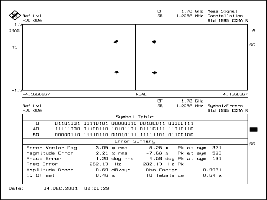
Figure 6. The MAX2361 EVM at +10dBm (measured at RFH0)..
Conclusion
This study of the MAX2361 has shown it's effectiveness and viability as an integrated solution for the Korean band wireless market. The MAX2361 achieves +10dBm output power while maintaining ACPR better than -55dBc in the Korean PCS band. The EVM recorded is 3.05% at +10dBm output power.
Related to this Article
Products
Obsolete
Complete Dual-Band Quadrature Transmitter
Obsolete
Complete Dual-Band Quadrature Transmitters
Obsolete
Complete Dual-Band Quadrature Transmitters

