The LTC1871 Achieves the Industry’s Highest Efficiency for Single-Ended Boost, Flyback and SEPIC Topologies
The LTC1871 Achieves the Industry’s Highest Efficiency for Single-Ended Boost, Flyback and SEPIC Topologies
by
Tick Houk
Sep 1 2001
Introduction
The LTC1871 is a general-purpose DC/DC controller IC optimized for use in boost, SEPIC and flyback converter applications. It provides flexible, high performance operation in a small MS10 package in order to extend the range of applications from single-cell, lithium-ion battery portable electronics up to high voltage, high power telecommunications equipment.
The LTC1871 is distinguished from conventional current mode controllers because the current control loop can be closed by sensing the voltage drop across the power MOSFET switch instead of across a discrete sense resistor, as shown in Figure 1a. This sensing technique provides the maximum efficiency possible for a single-ended, current mode converter. For applications where the drain of the power MOSFET exceeds 36V, or when more accurate control of the maximum current is important, the LTC1871 can also be used with a conventional sense resistor, as shown in Figure 1b.
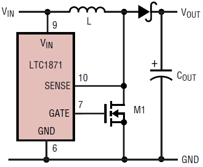
Figure 1a. Sensing on the drain of the power MOSFET
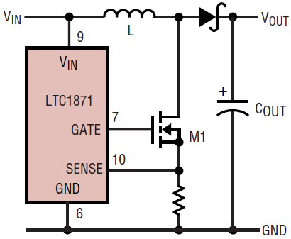
Figure 1b. Sensing on the source of the power MOSFET
Capable of operating with an input voltage from 2.5V to 32V (36V Abs Max), the LTC1871 also exhibits low quiescent current. When operating in continuous conduction mode (CCM), the quiescent current drawn by the IC is typically only 550µA plus the current required to switch the gate of the external power MOSFET (IQTOT = 550µA + QG • fOSC). In Burst Mode™ operation, at light loads, this total quiescent current (IQTOT) can drop to as low as 250µA. Finally, when the chip is in shutdown mode, with the RUN pin below 1.248V, the total quiescent current drops to a very low 10µA.
The operating frequency of the converter can be programmed over a 50kHz-to-1MHz range by means of a single resistor from the FREQ pin to ground. In addition, for systems where the switching frequency of the converter needs to be controlled by an external clock, the LTC1871 can be synchronized using the MODE/SYNC pin.
A Two-for-One Converter: High Efficiency 5V Output Boost Converter Operates from a 2.5V or 3.3V Input
Figure 2 illustrates a 5V output boost regulator that can operate from either a 2.5V or a 3.3V input supply. Having a single converter that can operate from different supply voltages greatly simplifies component purchasing and production control for volume manufacturers. This particular design takes advantage of the No RSENSE™ technology in order to maximize efficiency and reduce board space and total cost. Operating at a switching frequency of 300kHz enables the use of a small, inexpensive 1.8µH inductor from Toko. A Siliconix/Vishay SO-8 power MOSFET (the Si9426, which has a maximum RDS(ON) of 16mΩ at VGS = 2.5V and 13.5mΩ at VGS = 4.5V) and an International Rectifier surface mount diode (30BQ015) were chosen for the 2.0A output current level. A combination of Sanyo POSCAPs and low ESR Taiyo Yuden ceramic capacitors was used to reduce the output ripple to below 60mVP-P. It should be noted that the output current of a converter such as this can easily be scaled by the choice of the components around the chip without modifying the basic design.
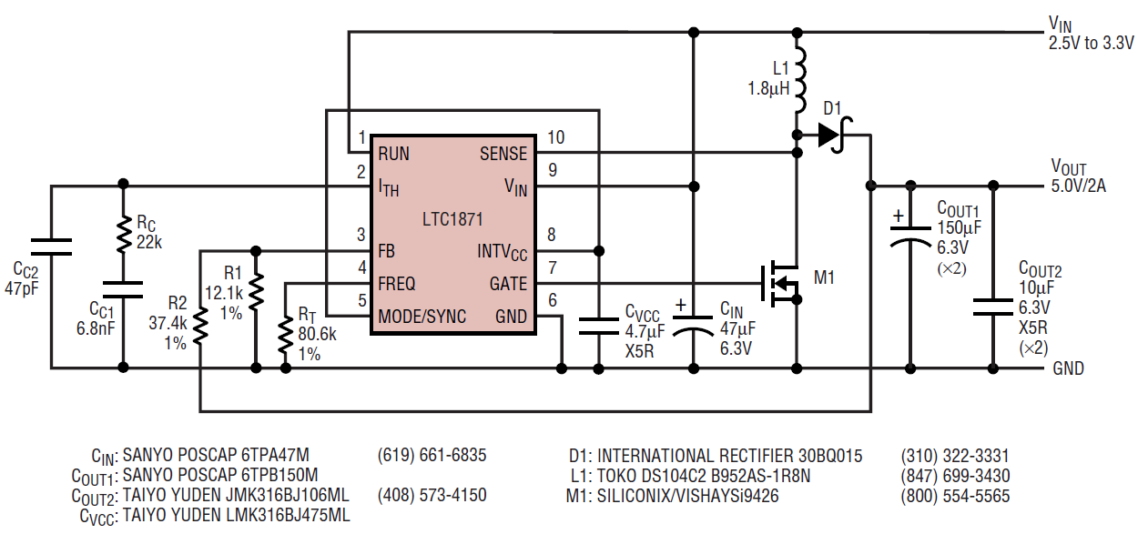
Figure 2. 2.5V to 3.3V input, 5.0V/2A output boost converter
Figure 3 illustrates the efficiency curves for this converter at input voltages of 2.5V and 3.3V; Figure 4 illustrates the load step response.
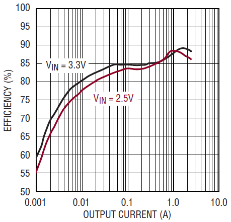
Figure 3. Efficiency vs input voltage for Figure 2’s converter
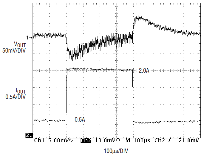
Figure 4. Load-step response for Figure 2’s converter
For applications where the maximizing the efficiency at very light loads (for example, < 100µA) is a high priority, the current in the output divider can be decreased to a few microamps and Burst Mode operation applied (the MODE/SYNC pin connected to ground). In applications where fixed frequency operation is more critical than low current efficiency, or where the lowest output ripple is desired, pulse-skipping mode operation should be used and the MODE/SYNC pin should be connected to the INTVCC pin. This allows discontinuous conduction mode (DCM) operation down to near the limit defined by the chip’s minimum on-time (about 175ns). Below this output current level, the converter will begin to skip cycles in order to maintain output regulation. Figure 5 shows the light load switching waveforms for Burst Mode and pulse-skipping mode operation for the converter in Figure 2 and Figure 6 illustrates the difference in measured efficiency.
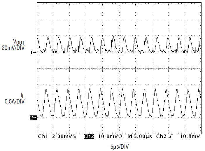
Figure 5a. Pulse-skip switching waveforms at light load for Figure 2’s circuit
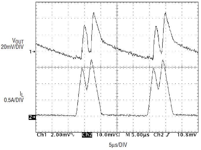
Figure 5b. Burst Mode switching waveforms at light load for Figure 2’s circuit
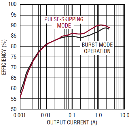
Figure 6. Efficiency vs operating mode for Figure 2’s converter
If synchronized operation is required, a logic-level clock signal can be applied to the MODE/SYNC pin. In this case, the turn-on of the power MOSFET will correspond to the rising edge of the clock signal. Because the internal slope compensation is increased by 30% during synchronized operation, setting the nominal operating frequency of the converter to 75% of the external clock frequency will result in the same net slope compensation.
The Fargo Converter: A 4.5V to 15V Input, 12V/1.5A Output SEPIC Converter
The primary advantage of the SEPIC converter is that the input voltage can be greater than or less than the output voltage. Such a converter is important in applications where the input voltage is either poorly regulated or experiences significant transients and the output voltage falls within this input range. A perfect example of such an environment exists in automotive, battery-supplied systems. Under normal conditions, the battery voltage in a car is approximately 13.7V. At very low ambient temperatures, such as are experienced in Fargo, North Dakota in the winter (–45°F without wind chill is not uncommon), the current required by the starter motor to crank a large V-8 engine can drag the battery voltage down below 5V. Certain systems in the car must be fully operational during this so-called cold cranking (for example, the engine control unit), hence a converter is needed that can maintain regulation under these low input conditions.
The SEPIC converter illustrated in Figure 7 can operate with a DC supply as low as 4.5V and also takes advantage of the No RSENSE technology in order to maximize efficiency. For this design, a coupled inductor from BH Electronics was chosen, along with International Rectifier’s IRF7811W power MOSFET (which has a maximum RDS(ON) of 12.5mΩ at VGS = 4.5V). A Taiyo Yuden ceramic capacitor was chosen for the DC coupling capacitor because of its low ESR and high RMS current capability. Figure 8 shows the efficiency for this converter at three input voltages and Figure 9 shows the typical load step response.
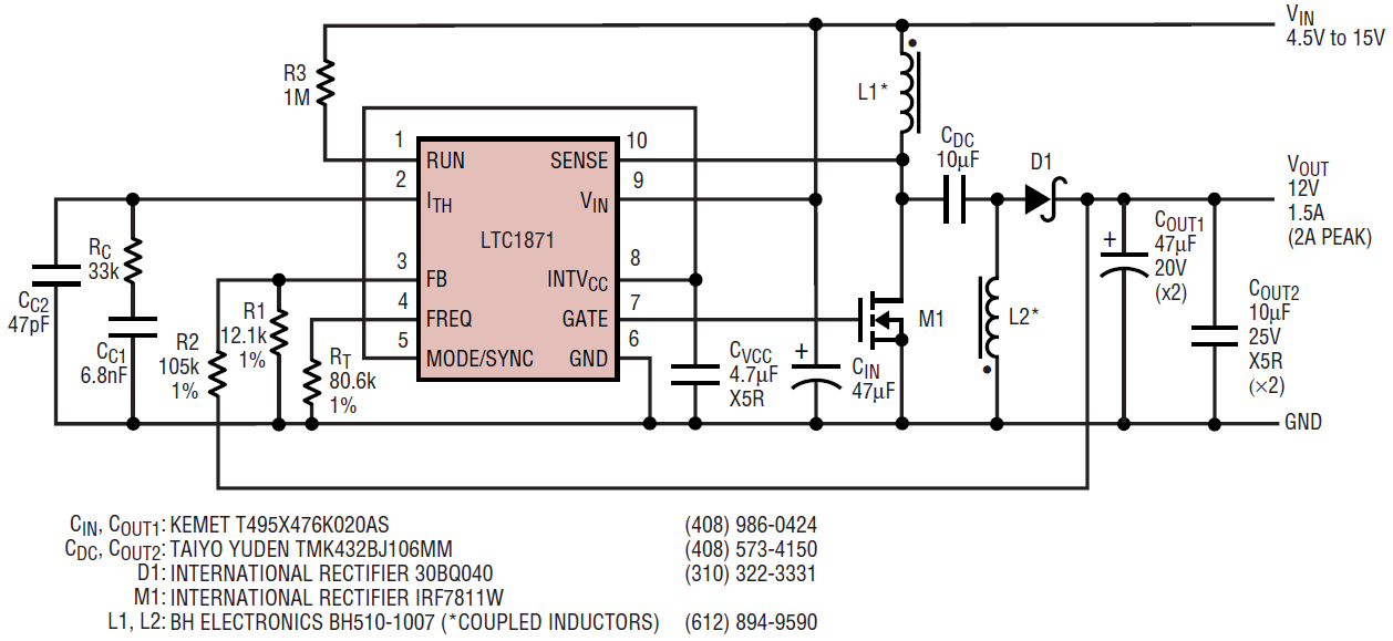
Figure 7. 4.5V to 15V input, 12.0V/2A output SEPIC converter
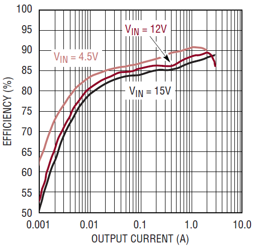
Figure 8. 12V output SEPIC converter efficiency vs input voltage and load current
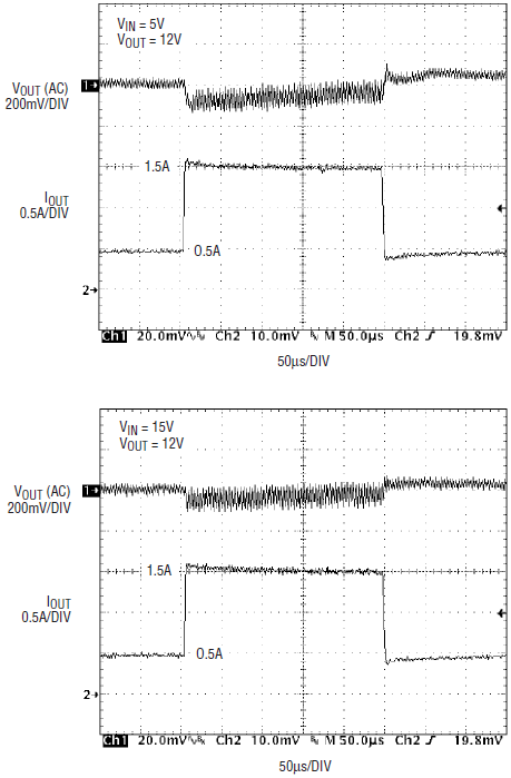
Figure 9. 12V output SEPIC converter load-step response; top, VIN = 5V; bottom, VIN = 15V
This design greatly benefits from the internal 5.2V low dropout regulator, or LDO, inside the LTC1871. Having such a wide input voltage range (4.5V–15V) would normally present problems for the gate drive to the power MOSFET. At low DC input voltages, any drop between the chip supply and the gate driver output would reduce the VGS of the MOSFET to as low as 3.3V (4.5V minus a typical drop of 1.2V through an NPN output stage), thereby requiring the use of a sublogic-level power MOSFET rated at a VGS of 2.5V. With the PMOS-output LDO in the LTC1871 and a strong CMOS gate driver, however, the full supply voltage is applied to the gate of the MOSFET, providing maximum efficiency and more flexibility in the choice of power MOSFETs.
At the other end of the input range, when the supply is 15V, the 5.2V LDO output in the LTC1871 limits the drive to the power MOSFET, thereby minimizing gate oxide stress and maximizing reliability.
A “SLIC” Flyback Power Supply
Figure 10 illustrates a multiple-output telecom power supply designed for use in subscriber line interface circuits (SLICs). The input to the SLIC power supply is some form of battery (lead acid or lithium-ion, for example) so that talk battery power can be provided to POTS (plain old telephone system) phones during an AC line failure (or rolling blackout). The output voltage is typically proportional to the distance the subscriber line runs from the local hub to a house or office, in order to compensate for the impedance of the loop. Multiple output supplies are used to supply groups of users at different distances from the hub.
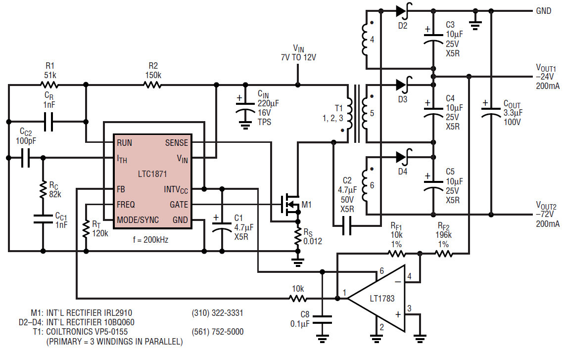
Figure 10. High power, dual-output SLIC supply
The –24V output of this supply uses one secondary winding in a capacitively coupled flyback configuration, whereas the –72V output uses the other two windings in a conventional flyback mode. The –24V output uses an LT1783 op amp to level-shift the feedback voltage, and the –72V output is obtained by stacking additional windings on the –24V output. A size 5, 6-winding Versapak transformer (VP5-0155) was used for convenience, with three windings connected in parallel on the primary to satisfy the primary current demand.
Unlike the previous, low voltage boost and SEPIC designs, which take advantage of the No RSENSE technology, this flyback converter places significant stress on the drain of the power MOSFET. As a result, a 100V BVDSS device is used (International Rectifier’s IRL2910), along with a conventional 12mΩ sense resistor in the MOSFET source (the absolute maximum voltage rating for the SENSE pin on the LTC1871 is 36V). The increase in losses due to this sense resistor are relatively small in this system (approximately 1%), due to the high input voltage.
For systems where control of the maximum output current is more important than overall efficiency, the use of a sense resistor can improve performance. The initial tolerance of a discrete sense resistor is commonly better than ±5%, whereas the initial tolerance of the RDS(ON) of a power MOSFET is typically ±20%–30%. In addition, the temperature coefficient of the discrete resistor can easily be an order of magnitude lower than for a power MOSFET (whose RDS(ON) increases approximately 50% from 25°C to 125°C).
The resistor divider formed by R1 and R2 is used to detect an undervoltage condition on the input supply in order to shut down the converter when the battery pack has discharged below 5.0V. For a falling input voltage (a discharging battery), the RUN pin on the LTC1871 is compared to an internal micropower 1.248V reference. If the RUN pin falls below this threshold, the chip shuts down and the quiescent current drops to 10µA in order to reduce the load on the battery. The hysteresis on the RUN pin comparator was chosen to be 100mV in order to compensate for the rise in the unloaded battery voltage (or other input supply) and to provide good noise immunity in general. In this particular design, the rising input start-up threshold is approximately 5.4V. The optional capacitor CR could be used to give the converter some ride-through capability for brief input transients.
Conclusion
The LTC1871 is a versatile control IC optimized for a wide variety of single-ended DC/DC converter topologies. Flexible, high performance operation is provided in a small, convenient MS10 package in order to improve efficiency, reduce the size and weight of the power supply, and reduce the total component and manufacturing cost.
About the Authors
Related to this Article
Products
PRODUCTION
1.25MHz, Over-The-Top Micropower, Rail-to-Rail Input and Output Op Amp in SOT-23
PRODUCTION
Wide Input Range, No RSENSE™ Current Mode Boost, Flyback and SEPIC Cont...


