Reference Design for a Powered-Device (PD) Module Based on the MAX5941B PWM Controller
This application note presents an IEEE 802.3af-compliant, powered-device (PD) module for power-over-Ethernet (PoE) applications. Based on the MAX5941B PoE interface/PWM controller, this module provides the PD with a detection signature, a configurable classification signature (optional), programmable undervoltage lockout (UVLO), and an isolation switch with programmable inrush-current control.
The MAX5941B PD module is assembled on a 12cm² PCB and includes hot-swap power switching, a DC-DC converter, and a pair of ORing diode bridges for compatibility with an external 12V adapter. In short, it provides all the functions necessary to implement a DC-DC, fixed-frequency, isolated power supply for PDs, such as IP phones, wireless access nodes, and security cameras.
Typical Application
The MAX5941B PD module can be used in numerous applications. Figure 1 illustrates a typical application in which the data outputs from the switch are connected to the inputs of a midspan. The midspan then adds power to the data on each output that supports PoE.
In this example, port 1 is connected to an Ethernet camera and port 2 is connected to a wireless access point. When the midspan is switched on (or when the device is connected), the midspan checks each output for a PoE signature. The module identifies the peripherals on ports 1 and 2 as PoE-enabled devices, and the midspan supplies both data and power to these peripherals.
The midspan continuously monitors each output to see if a PoE-enabled device has been added or removed. Since the other ports in this example do not have a PoE signature, the midspan only passes data through to the connected peripherals.

Figure 1. In a typical application, the data outputs from the switch are connected to a midspan, which adds power to the data to provide power over Ethernet.
Features
- IEEE 802.3af compliant
- 36V to 60V input voltage range
- 12V/1A output
- No minimum load requirement
- Small SIL package size
- Low output ripple and noise
- High-efficiency powered device
- No external capacitor required
- Adjustable output voltage
- Low cost
- 1500V isolation (input to output)
- On-board ORing diode used with an external 12V adapter
Pin Description

Figure 2. Pin assignment
| Pin Number | Name | Description |
| 1 | VA1 | Rx Input (1) This input pin is used in conjunction with VA2 and connects to the center tap of the transformer connected to pins 1 and 2 of the RJ45 connector (Rx)—it is not polarity sensitive. |
| 2 | VA2 | Tx Input (2) This input pin is used in conjunction with VA1 and connects to the center tap of the transformer connected to pins 3 and 6 of the RJ45 connector (Tx)—it is not polarity sensitive. |
| 3 | VB1 | Direct Input (1) This input pin is used in conjunction with VB2 and connects to pins 4 and 5 of the RJ45 connector—it is not polarity sensitive. |
| 4 | VB2 | Direct Input (2) This input pin is used in conjunction with VB1 and connects to pins 7 and 8 of the RJ45 connector—it is not polarity sensitive. |
| 5 | CP1 | Class Programming (1) Connecting an external resistor to CP2 will change the current class of the module. With no resistor fitted the module will default to Class 0. |
| 6 | CP2 | Class Programming (2) Connecting an external resistor to CP1 will change the current class of the module. With no resistor fitted the module will default to Class 0. |
| 7 | GND | Ground The ground return for the output. |
| 8 | VOUT | DC Output This pin provides the regulated output voltage from the DC-DC converter. |
| 9 | ADJ | Output Adjust The output voltage can be adjusted from its nominal output by connecting an external resistor from this pin to either the VOUT pin or GND pin. |
| 10 | N.C. | No Connection This pin is not connected internally. |
Power Classification
Power classification is an optional method for the PD to indicate its power requirements to the power-sourcing equipment (PSE). The MAX5941B module allows the current class to be externally programmed by connecting a resistor between the CP1 and CP2 pins, as shown in Figure 3. If no resistor is fitted, the module will default to Class 0. Table 2 provides a full list of programming resistor values.
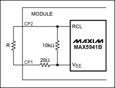
Figure 3. To set the power classification, connect a resistor between pins CP1 and CP2
| Class | Programming Resistance (Ω) | Minimum Power (W) | Maximum Power (W) |
| 0 | Do not fit | 0.44 | 12.95 |
| 1 | 770 | .44 | 3.84 |
| 2 | 388 | 3.84 | 6.49 |
| 2 | 388 | 3.84 | 6.49 |
| 3 | 242 | 6.49 | 12.95 |
| 4 | 161 | Reserved | Reserved |
Output Adjustment
The MAX5941B PD module has an ADJ pin to trim the output voltage up or down from its nominal value. To adjust the output voltage, connect a resistor between the ADJ pin and either the GND pin or the VOUT pin (Figure 4). Equations 1 and 2 calculate the resistor values required to achieve the desired trimmed-up and trimmed-down output voltages.


where VTRIM_UP is the desired trimmed-up output voltage and VTRIM_DOWN is the desired trimmed-down output voltage.

Figure 4. To adjust the output voltage, connect a resistor between ADJ and GND (trim up) or ADJ and VOUT (trim down)

Figure 5A. The trimmed-up output voltage curve
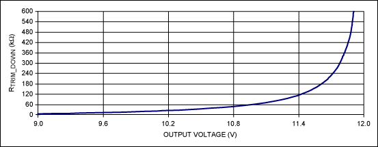
Figure 5. The trimmed-down output voltage curve
Typical Connections with an External 12V Adapter
Conventionally, the PD is used simultaneously with an adapter, and a diode is connected in series at each output as shown in Figure 6.

Figure 6. In the conventional solution, the powered device is connected to an adapter, with a diode placed in series at each output
For the MAX5941B PD module, the output diode D1 is assembled internally. If the PD is used independently, replace the diode with a 0Ω resistor to improve efficiency. Figure 7 shows the placement of the ORing diode D1 on the board.

Figure 7. The location of the internal diode D1 on the MAX5941B PD module
The module only requires one external capacitor, as shown in Figure 8; minimally, a 1µF ceramic capacitor is recommended.

Figure 8. Typical connection diagram showing the external capacitor connected between GND and VOUT.
Electrical Characteristics
| Parameter | Min | Typ | Max | Units |
| DC Supply Voltage | -.3 | 60 | V | |
| DC Supply Voltage Surge for 1ms | -.6 | 80 | V | |
| Storage Temperature | -40 | +100 | °C |
Stresses beyond those listed under "Absolute Maximum Ratings" may cause permanent damage to the module. These are stress ratings only, and functional operation of the module at these or any other conditions beyond those indicated is not implied. Exposure to absolute maximum ratings conditions for extended periods may affect the module's reliability.
| Parameter | Min | Typ | Max | Units |
| Input Supply Voltage | 36 | 48 | 60 | V |
| Undervoltage Lockout | 30 | 36 | V | |
| Operating Temperature | -40 | 25 | +85 | C° |
| Parameter | Min | Typ | Max | Units |
| Nominal Output Voltage (Without the ORing Diode) | 11.76 | 12 | 12.24 | V |
| Output Current | 0 | 1 | A | |
| Output Ripple and Noise | 250 | mV | ||
| Efficiency Without the ORing Diode (48V Input, 1A Output) | 85 | % | ||
| Efficiency with the ORing Diode (48V Input, 1A Output) | 82 | % | ||
| Isolation Voltage | 1500 | V |
Waveforms

Figure 9. Output ripple and noise

Figure 10. Startup and shutdown

Components List
| Designation | Qty | Description |
| C1, C2, C6, C17 | 4 | 10µF 25V ceramic capacitor 1206 TDK C3216X5R1E106K MURATA GRM31CR61E106KA12 |
| C3 | 1 | 6800pF 100V ceramic capacitor 0603 TDK C1608X7R2A682K |
| C4 | 1 | 100pF 50V ceramic capacitor 0603 |
| C4 | 1 | 100pF 50V ceramic capacitor 0603 |
| C5, C7, C23 | 1 | 0.1µF 50V ceramic capacitor 0603 |
| C9 | 1 | 10µF 100V aluminium electrolytic capacitor SANYO 100CE10FS |
| C9 | 1 | 10µF 100V aluminium electrolytic capacitor SANYO 100CE10FS |
| C10 | 1 | 1000pF 1.5kV ceramic capacitor 1808 TDK C4520X7R3D102K |
| C12, C25 | 2 | 0.1µF 100V ceramic capacitor 1206 TDK C3216X7R2A104K |
| C13 | 1 | 220µF 25V aluminium electrolytic capacitor SANYO 25CE220FSA |
| C14 | 1 | 1000pF 100V ceramic capacitor 0805 TDK C2012X7R2A102K |
| C19 | 1 | 2.2µF 10V ceramic capacitor 0603 MURATA GRM188R61A225KE34 |
| C22 | 1 | 680pF 50V ceramic capacitor 0603 |
| C28 | 1 | 4700pF 50V ceramic capacitor 0603 |
| D1, D2 | 1 | Bridge rectifier DIODES HD01-T |
| D4, D6 | 2 | Diode 200mA 250V SOD323 DIODES BAV21WS |
| D5, D13 | 2 | 60V Schottky rectifier SMA DIODES B360A |
| D7 | 1 | SMT LED Lamp 0603 FAIRCHILD QTLP600C-Y |
| D8 | 1 | Transient Voltage Suppressor DIODES SMAJ54A |
| R1 | 1 | 20Ω ±1% resistor 0603 |
| R5 | 1 | 270mΩ ±1% resistor 1206 |
| R9 | 1 | 470Ω ±1% resistor 0603 |
| R10 | 1 | 10Ω ±1% resistor 1206 |
| R11, R17 | 2 | 10kΩ ±1% resistor 0603 |
| R12 | 1 | 20kΩ ±1% resistor 0603 |
| R14 | 1 | 25.5kΩ ±1% resistor 1206 |
| R15 | 1 | Not Used |
| R16 | 1 | 0Ω ±1% resistor 1206 |
| R18 | 1 | 1kΩ ±1% resistor 0805 |
| R22 | 1 | 9.53kΩ ±1% resistor 0603 |
| R23 | 1 | 2.49kΩ ±1% resistor 0603 |
| R24, R31 | 2 | 2.5kΩ ±1% resistor 0603 |
| R25, R27 | 2 | 1kΩ ±1% resistor 0603 |
| R26 | 1 | 4.75kΩ ±1% resistor 0603 |
| R28 | 1 | 33kΩ ±1% resistor 0805 |
| R30 | 1 | 4.7Ω ±1% resistor 0805 |
| Q1 | 1 | MOSFET 150V SO-8 IR IRF7465TR |
| U2 | 1 | IC Optocoupler NEC PS2801-1-F4-R-A |
| U3 | 1 | IC VREF 2.5V 0.4% SOT-23 AAC AZ431AN-A |
| U5 | 1 | PWM controller for PD MAXIM MAX5941BESE |
| R30 | 1 | Transformer NP:NS:NB = 35:16:20 LP = 122µH GA3271-AL Coilcraft |
Transformer Design
| Parameter | Conditions | Value |
| Electrical Strength | 50Hz 1 minute, from pins 1–3, 10–12 to pins 5–8 | 1500VRMS |
| Primary Inductance | Pins 1, 12; all windings open. Measure at 275kHz | 120µH ±10% |
| Primary Leakage Inductance | Pins 1, 12; rest of pins shorted. Measure at 275kHz | 3µH (max) |
| Item | Description |
| 1 | Core: EFD15, PC40. Manufacturer: TDK |
| 2 | Bobbin: EFD15 coil former (SMD), 12 pins |
| 3 | Tape: 8.9mm wide insulation tape |
| 3 | Tape: 8.9mm wide insulation tape |
| 3 | Tape: 8.9mm wide insulation tape |
| 4 | Magnet Wire: .25mm diameter with 150°C |
| 5 | Magnet Wire: .27mm diameter with 150°C |
| 6 | Magnet wire: 0.10mm diameter with 150°C |
| 7 | Varnish |
| Note | All wires include insulation |

Figure 13. Transformer building diagram
| Step | Description |
| Primary NP1 | Start at pin 1. Wind 35 turns of item 4 in approximately 1 layer. Finish on Pin 12 |
| Insulation | Use 1 layer of item 3 for insulation |
| 12V Winding | Start at pins 6 and 5. Wind 16 turns of 2 parallel strands of item 5. Finish at pins 7 and 8 |
| Insulation | Use 1 Layer of Item 3 for Safety Insulation |
| Primary NP2 | Start at pin 2. Wind 35 turns of item 4 in approximately 1 layer. Finish on pin 11 |
| Insulation | Use one layer of item 3 for safety insulation |
| Bias Winding | Start at pin 3. Wind 20 turns of item 6. Spread turns evenly across bobbin. Finish at pin 10 |
| Outer Wrap | Wrap Wwndings with 2 layers of item 3 |
| Final Assembly | Assemble and secure core halves. Varnish impregnate with item 9 |
Related to this Article
Products


