Precision Fully Differential Op Amp Drives High Resolution ADCs at Low Power
Precision Fully Differential Op Amp Drives High Resolution ADCs at Low Power
by
Kris Lokere
Jan 1 2014
The LTC6362 op amp produces differential outputs, making it ideal for processing fully differential analog signals or taking a single-ended signal and converting it to fully differential. Many alternative op amps of this fully differential nature are optimized for very high speed operation,resulting in high power consumption and lack DC accuracy. The LTC6362 is unique in that it features differential outputs, low power consumption and accurate DC offset voltage (see Table 1).
| Supply Current | 1mA |
| Maximum Offset Voltage | 200μV |
| –3dB Bandwidth | 34MHz |
| Input Noise Density |
3.9nV/√Hz |
| Input Voltage Range | Rail-to-Rail |
| Output Voltage Range | Rail-to-Rail |
| Supply Voltage | 2.8V – 5.25V |
Why Fully Differential Analog Signals?
An analog signal is usually represented as one signal measured with respect to a fixed potential such as ground, also known as a single-ended signal. But there are times when it is better, or necessary, to make the analog signal fully differential. Fully differential means that two nets each vary with signal. Whenever one voltage goes higher, the other voltage goes lower by the same amount. The analog signal is defined as the voltage difference between these two nets.
One benefit of fully differential signal processing is that it can reduce sensitivity to external interference, such as power supply noise, ground bounce or electromagnetic interference (EMI). For example, if power supply noise couples equally to both conductors that carry your fully differential signal, then the difference signal may remain undisturbed.
Another benefit of fully differential signal processing is that you can squeeze more signal into a given supply voltage range. For example, in a system that is powered from a single 5V supply, a traditional single-ended signal can vary at most 5V. But a fully differential signal can vary from –5V to 5V, for 10VP–P. That is because either of the two nets can be higher or lower than the other, which effectively doubles the signal swing. For a given noise floor, doubling the maximum signal swing results in a 6dB improvement in the signal-to-noise ratio (SNR).
Finally, some semiconductor components mandate, per the data sheet, that you provide a fully differential signal into the input. This fully differential input requirement is near universal for ADCs that convert at a high sample rate (e.g., pipeline ADCs at >10Msps) as well as for ADCs that achieve very high resolution, high linearity and low noise (e.g., SAR ADCs at ≥18 Bit and ≥100dB SNR). Therefore, to use those components, you have no choice but to convert your analog signal to fully differential at some point in your signal chain.
How Does It Work?
Let’s take a closer look at how a differential op amp works. Just like a regular op amp, it has two inputs, but unlike a regular op amp, it also has two outputs, labeled –OUT and +OUT. A regular op amp features high open-loop gain between the differential input and the one output; a fully differential op amp features high open-loop gain between the differential input and the differential output.
Feedback should also be applied differentially. Figure 1 shows four external resistors feeding a portion of the differential output back into the differential input. Just like in a regular op amp, the high open-loop gain combined with the feedback effectively forces the two inputs to bias at nearly identical voltages, often called “virtual ground.” Circuit analysis is based on the concept of virtual ground. The differential gain of the circuit is equal to
 |
(1) |

Figure 1. Four external resistors apply feedback around the differential op amp.
Equation 1 shows that the differential output voltage depends only on the difference between the two inputs, regardless of the absolute voltage on each input. To convert a single-ended input to a differential output, simply connect one of the inputs to ground.
Although Equation 1 explains how to determine the differential output voltage, it neither reveals the voltages of each output, nor the average voltage of the two output nodes. For the LTC6362, the instantaneous average of the two outputs (also called the output common mode voltage) is independent of the input voltage, but instead is user-determined by the voltage on the VOCM pin.
 |
(2) |
If both the average of the two outputs and the difference of the two outputs are known, equations 1 and 2 can be used in as a linear system of two equations and two variables to determine the value of each output.
Figure 2 shows how the LTC6362’s differential output can be governed by Equation 1 while the common mode output is held at VOCM. The LTC6362 features an additional feedback loop with a separate error amplifier. Two internal resistors measure the instantaneous average of the two outputs, and feed that into the error amplifier with its other input tied to the VOCM pin. The output of the error amplifier is connected to the main amplifier in such a way that it attempts to move each of the op amp outputs higher or lower depending on how the error amplifier is driven. (You can think of it as extra current injected into a mirror driving the main op amp’s output stages). When this common mode feedback loop closes to a stable operating point, it ensures that the average of the two outputs is equal to VOCM, while the difference between the two outputs is controlled by the differential feedback around the main op amp.

Figure 2. Inside the LTC6362 differential op amp is an additional feedback loop and error amplifier, providing common mode feedback (CMFB).
How Do You Hook It Up?
Once you understand that the differential gain of the circuit is simply set by the resistor ratio RF/RI, and the output common mode is independently set by the voltage on VOCM, it is easy to apply the LTC6362 for a variety of signal translations. Figures 3 and 4 show some typical examples.

Figure 3. Translating a 0V–5V input signal to 9VP–P differential output.

Figure 4. Translating a ±10V input signal to a 9VP–P differential output.
You may notice that in the example of Figure 4, we let the input signal swing below ground, even though the op amp is not powered from a negative supply rail. This works thanks to the divider action of the feedback resistors and the LTC6362’s rail-to-rail input stage. The input pins of the op amp itself are fully specified to operate for any voltage up to and including either of the supply rails. You can analyze or simulate any of the example circuits and see that the voltage at the op amp inputs does not need to go below ground even though the voltage at the signal input does.
Low Noise and How Do You Calculate It?
One key advantage of differential signal processing is the potential to double the signal-to-noise ratio of the system. So let’s take a closer look at how to analyze the noise performance of a differential op amp such as the LTC6362.
The op amp specifies an input-referred noise density of just under 4 nV/√Hz. This can be modeled as a noise voltage source in series with one of the inputs. The effect of that noise on the output of the circuit is the inverse of the feedback ratio. For example, if all resistors are equal value, then half of the output voltage is fed back into the op amp inputs, and the op amp input noise appears times a factor of two at the output.
In addition, each of the four feedback resistors contributes noise at √4kTR. You need to combine the contributions of these noise sources. For the example with RF = RI = 1k, this results in a total output noise of 12nV/√Hz.
Once you know the total output noise density of the circuit, you can calculate RMS noise by integrating over the bandwidth of interest. As usual, the lower the bandwidth, the more you time-average the noise, and therefore the lower the total observed noise becomes. For example, the noise bandwidth of a 1MHz single-pole filter is 1.57MHz. Integrating the 12nV/√Hz noise density over that bandwidth results in approximately 15μVRMS of total noise.
You can calculate the maximum SNR of the circuit by dividing the maximum signal by the noise. The LTC6362 features rail-to-rail outputs which, on a single 5V supply, result in an almost 10VP–P differential output swing. If you convert that to RMS (3.5VRMS) and divide by the noise (15μVRMS), you get an SNR of more than 233,000 or 107dB in this 1MHz of noise bandwidth. The 107dB figure makes the LTC6362 a good match for the LTC2378-20 20-bit SAR ADC, which features 104dB SNR, and requires fully differential input drive.
Driving a 20-bit SAR ADC
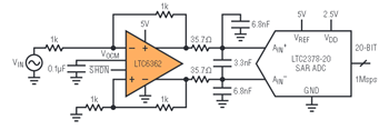
Figure 5 shows how to use the LTC6362 to drive the LTC2378-20, a 20-bit SAR ADC sampling at 1Msps. The LTC6362 takes a single-ended input signal and converts it to a fully differential output, just as the ADC specifies.

Figure 5. The LTC6362 driving the 20-bit 1Msps LTC2378-20 ADC.
The RC filter network in between the amplifier and the ADC serves several purposes. First, the filter network reduces the amount of wideband noise that would enter the ADC. For an ADC sampling at 1Msps, the Nyquist criterion says that any signals above 500kHz would alias and become indistinguishable from lower frequency signals. That is true for wideband noise as well, so there is no reason to let the wideband noise enter into the ADC. Second, the capacitors serve as a charge reservoir to absorb charge kick-back from the ADC’s internal sampling capacitors. Every time that the ADC finishes the previous conversion, it reconnects discharged sample capacitors (about 45pF) to the amplifier circuit. By placing a much larger reservoir capacitor at the ADC inputs, you reduce the voltage excursion caused by these sample capacitors.
The period of time after the ADC has finished a conversion and before it starts the next conversion is called the acquisition time. This is the period of time during which the sample capacitors remain connected to the amplifier circuit.
Ideally, during this time, the RC network fully settles to within the resolution of the ADC. In practice, you may make a trade-off between wideband noise and settling time. Fortunately, the LTC2378-20 ADC charge kickback is relatively linear, ensuring excellent linearity, even when the sample capacitors have not yet fully settled to their final value.
The combined performance of the circuit shown in Figure 5 achieves an SNR of 103dB and THD of 107dB. This is breakthrough performance for a data acquisition system at 1Msps. Best of all, the LTC6362 eases the burden of providing a fully differential input into the ADC with a precise common mode. Indeed, the input to this circuit is a traditional single-ended analog signal. To configure the circuit for other input ranges, simply choose appropriate external resistors, as shown in the earlier figures.
Driving a 25Msps Pipeline ADC
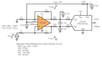
High speed pipeline ADCs typically require that their inputs be driven fully differential. Figure 6 shows how to take a single-ended analog signal with frequency content from DC to about 1MHz and over sample it at 25Msps.

Figure 6. LTC6362 drives the LTC2160 16-bit high speed pipeline ADC.
Here, the LTC6362 converts the signal to differential outputs. The LTC2160 ADC wants the common mode of its inputs to be at 0.9V. You achieve this by connecting the VCM pin of the ADC to the VOCM pin of the amplifier. Few differential op amps are capable of supporting this low of a common mode voltage this low while achieving the performance of the LTC6362. The SNR of the circuit is 77dB, equal to the SNR spec of the ADC, and quite impressive given the low total power consumption of 45mW for the ADC and 3mW for the amplifier.
Differential Line Driver
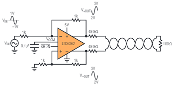
Sometimes you need to transport an analog signal over a relatively large distance from one PCB to another. A good way to do that is by using a differential twisted pair, because it provides immunity to noise coupling and other interference. As previously discussed, the LTC6362 can convert a traditional single-ended signal to fully differential, in this case driving it over the differential line, as shown in Figure 7.

Figure 7. LTC6362 conditions a signal to drive across a differential twisted pair.
Differential Active Filter
An op amp-RC active filter can be used to produce a lowpass filter with multiple poles, and a cutoff frequency that is relatively well established. Circuit examples that do this with a traditional op amp are readily available. The LTC6362 is can be used to fully implement such filters differentially.
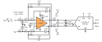
Figure 8 shows an example of a 4-pole 50kHz lowpass filter. In this example, the LTC6362 performs three functions at once: it converts a single-ended input signal to fully differential, it forms a 4-pole lowpass filter and it drives a high performance ADC (in this example, the 16-it 20Msps LTC2380-16).

Figure 8. Configuring the LTC6362 as a differential active-RC filter.
Not all differential op amps are capable of being used in this way. The feedback capacitors create a high frequency short directly from the op amp output to the op amp input, meaning that the feedback factor at high frequencies is much stronger than in a circuit with feedback resistors. If the op amp does not have sufficient phase margin, oscillations or ringing occur. In contrast to a traditional op amp, LTC6362 performs admirably in this configuration.
Conclusion
The LTC6362 is a capable and versatile differential op amp. Accurate DC specifications, low power and rail-to-rail operation enable it to drive a variety of high performance ADCs that require differential signals, as well as perform active filtering or drive differential cables.
About the Authors
Kris Lokere is a strategic applications manager for signal chain products, joining ADI as part of the merger with Linear Technology. Kris enjoys architecting systems that combine technologies from multiple product lines. I...


