POL μModule DC/DC Converter Operates from Inputs Down to 1.5V, Delivering Up to 15A Output, Without an Auxiliary Bias Supply
POL μModule DC/DC Converter Operates from Inputs Down to 1.5V, Delivering Up to 15A Output, Without an Auxiliary Bias Supply
Oct 1 2010
The LTM4611 is a low profile μModule step-down switch mode DC/DC converter in a compact 15mm × 15mm × 4.32mm LGA surface mount package. The switching controller, MOSFETs, inductor and support components are housed in the package, so design is reduced to selecting a few external components. The LTM4611 operates from an input voltage of 1.5V to 5.5V (6V, absolute maximum), making it suitable for a variety of power architectures—particularly data storage and RAID (redundant array of independent disks) systems, ATCA (advanced telecommunications computing architecture) and networking cards—where one or several commonly bussed voltages are 5V, 3.3V, 2.8V, and/or 2.5V.
While it is uncommon to see bus voltages lower than 2.5V due to the distribution losses (voltage drops) associated with relatively high bus currents, the ability of the LTM4611 to deliver full power to its load from a 1.5V input is particularly advantageous in applications where load voltage(s) must be precisely regulated even as momentary or sustained electrical events induce input-bus line-sag. Transient events on the system bus can occur normally due to the operation of motors, transducers, defibrillators or an uptick in microprocessor activity. Fault events on a system’s distributed bus may leave the bus voltage compromised, but still above 1.5V. The LTM4611’s ability to deliver full power from as low as 1.5V input allows it to be considered for mission-critical medical and industrial instruments that have the highest standards for uptime and bus-sag ride-through capability. Precision-regulated power can even be provided by the LTM4611 to its load during so-called “dying-gasps”—sudden, unexpected loss of system power, such as those monitored by utility smart meters—where it is highly desirable to be able to operate from the decaying voltage provided by backup-batteries or supercapacitors for as long as possible.
There is another advantage in the LTM4611’s ability to operate from as low as 1.5V: as the number of rails increases in today’s power system, so are the number of layers of copper in printed circuit boards (PCBs) required to route (distribute) the power effectively to the load. Consider a hypothetical example: it can be difficult to impossible to route a distributed 5V rail to both 5V-to-1.5V and 5V-to-1.2V DC/DC converters without increasing the number of layers of copper in the PCB. Alternatively, one LTM4611 could convert the 5V rail to a distributed 1.5V copper plane, while another LTM4611 could efficiently convert the 1.5V bus voltage to 1.2V at the POL. The resulting total solution size on the motherboard could be quite compelling, while eliminating the need to route 5V potential to an entire section of the PCB. The option to minimize the number of layers of copper in the manufacture of the PCB has potential for cost and material savings, and associated benefits to PCB yield in mass-production and PCB reliability.
Brains and Brawn
The muscle behind the LTM4611 is a buck-converter topology that steps down its input voltage to deliver as low as 0.8V, up to 15A continuous, to its output. A voltage drop less than 0.3V from input-to-output and at 15A load is achievable, with proper selection of input-power-source (dynamic characteristic and transient load response) and local bypass capacitance.
Self-Generated Bias Supply
Another noteworthy feature is that the LTM4611 does not require an auxiliary bias supply to power its internal control IC or MOSFET-drive circuitry; it generates its own low power bias from the input-source supply. The LTM4611 employs a fixed-frequency peak-current-mode control buck-converter scheme, operating at 500kHz by default. The switching frequency can be adjusted between recommended values of 330kHz to 780kHz with resistor-pin strapping to the PLLFLTR/fSET pin of the LTM4611, or synchronized between 360kHz and 710kHz to a clock signal applied to the MODE_PLLIN pin.
Current Sharing of Multiple Supplies for 60A or More
Current sharing of four modules is supported for solutions up to 60A output. More modules can be paralleled for even higher output current—call the factory for details. Current mode control makes current sharing of modules especially reliable and easy to implement, and ensures module-to-module sharing of current during start-up, transient and steady-state operating conditions.
This is in contrast to many voltage mode modules, which achieve current-sharing by employing either master-slave configurations or by using “droop-sharing” (also called “load-line sharing”). Master-slave configurations can be vulnerable to nuisance overcurrent-tripping during start-up and transient load conditions, while droop-sharing results in compromised load regulation specifications while offering little assurances of good module-to-module current matching during transient load steps.
The LTM4611 typically provides better than 0.2% load regulation from no load to full load—0.5% maximum over the full internal module temperature range of −40°C to 125°C.
Easy POL Application: 1.8V–5.5V Input to 1.5V Output at 15A
The block diagram in Figure 1 shows the LTM4611 operating from 1.8V-to-5.5V input and delivering 1.5V output at 15A. The output voltage is programmed by a single resistor from VFB to GND. The control loop drives the power MOSFETs and output voltage such that VFB is equal to the lesser of 0.8V or the voltage on the TRACK/SS pin. A soft-start capacitor, CSS, on the TRACK/SS pin programs the start-up rate of the LTM4611’s output when the module’s RUN pin exceeds 1.22V (±10%). CSS assures monotonic output voltage waveform start-up and supports smooth power-up into pre-biased output voltage conditions. A resistor-divider from another rail can be applied to the TRACK/SS pin to program coincident or ratiometric tracking of the LTM4611’s output rail to the reference rail. This is a handy feature when powering digital devices with stringent rail-tracking requirements during system power-up and power-down.

Figure 1. Simplified block diagram of the LTM4611, and typical application.
Programmable Undervoltage Lockout with Programmable Rising and Falling Thresholds
The resistor-divider (R1/R2) from the input-source (VIN) to the RUN pin of the LTM4611 programs the UVLO (undervoltage lock out) rising and falling thresholds of the DC/DC μModule converter. This ensures that the converter does not draw current from VIN until the input (bus) voltage exceeds the minimum DC voltage, and also programs the hysteresis voltage—the amount of input voltage sag at which the DC/DC converter ceases to regulate (shuts off power to) its output. For minimum component-count and default 80mV hysteresis, connect RUN to VIN, directly. The use of R1 without R2 yields the minimum possible start-up voltage (~1.22V, typical) and allows programming of the turn-off hysteresis.
The role of UVLO is important in all power supply conversion applications, including ultralow VIN DC/DC converter applications that operate at high duty-cycle. Input-referred transient currents that flow as a result of the DC/DC converter responding to transient load steps on its output must be absorbed by the source supply and the input (bus) capacitance, where the combination of a sluggish source supply and insufficient bus bypass capacitance is a recipe for undesirable power supply motor boating during power-up into heavy loads.
Easy Loop Compensation
The LTM4611 control loop is internally compensated to yield a stable system with a wide assortment of output capacitors. Nevertheless—especially when using low leakage, low ESR, high reliability X5R- or X7R-material ceramic capacitors on the output—transient response can be further improved with a small signal capacitor from VOUT to VFB (CFF), and/or a small signal capacitor from VFB (CP) to SGND may be warranted to guarantee control loop stability, accounting for ceramic capacitor value variation and ESR variation over age, temperature, and capacitor process.
The LTM4611 data sheet and Linear’s simulation design and modeling tools, such as LTspice® and the LTpowerCAD™, take the guesswork out of the loop-stability and transient-load response optimization process. Figure 2 shows transient load response of the LTM4611 for some typical 1V output and 3.3V output applications and data sheet-endorsed ceramic-only output capacitance.

Figure 2. A sampling of the LTM4611’s output voltage transient load responses.
Remote Sensing for Accurate POL Regulation
Routinely, high current low voltage FPGAs, ASICs, μPs, etc., require extremely accurate voltages of ±3% of nominal VOUT (or better) regulated exactly at the POL terminals (e.g. VDD and DGND pins). To meet this regulation requirement where it is hardest to do so—for low output voltages (≤3.7V)—the LTM4611 provides a unity gain buffer for remote sensing of the output voltage at the load’s terminals.
Voltage drops across the VOUT and GND copper planes in the PCB are an unavoidable result of resistive distribution losses physically between the module and the load. In Figure 1, it can be seen that the differential feedback signal across the POL (VOSNS+ minus VOSNS−) is reconstructed at DIFF_VOUT with respect to the module’s local ground, SGND, thus allowing the control loop to compensate for any voltage drop in the power-delivery path between the module’s output pins and the POL device.
The LTM4611 includes an output voltage power good (PGOOD) indicator pin that supplies a logic high open-drain signal when output voltage is within ±5% of nominal VOUT; otherwise, PGOOD pulls logic low. The LTM4611 provides fold-back current-limiting to protect itself and upstream power sources from fault conditions on its output. The LTM4611 also includes an overvoltage protection feature: when the output voltage exceeds 107.5% of nominal, the internal low side MOSFET is turned on until the condition is cleared.
Light Load Operating Modes to Improve Efficiency or Minimize Ripple
Lastly, the LTM4611 supports forced continuous mode (FCM), pulse-skipping mode (PSM) and Burst Mode® operation schemes, depending on the efficiency and ripple requirements of the application at light loads. These modes are selected by terminating the MODE_PLLIN to GND, pulling it to INTVCC or leaving it floating, respectively. At relatively heavy load currents (>3A), one does not see any difference in module behavior between these three modes—the difference is in light load performance.
At light loads (<3A), in FCM, the power MOSFETs are forced to operate synchronously every switching cycle—energy flow between input source and output load is bidirectional—to minimize inductor ripple current and therefore output voltage ripple. In pulse-skipping operation, energy flow is unidirectional—from input to output, only—and the top MOSFET can turn off for multiple switching cycles at light loads. PSM allows slightly higher efficiency at lighter loads (<3A)—due to decreased switching losses—and yields output voltage ripple and transient load response on par with FCM operation. Pulse-skipping mode accomplishes what is also referred to as “diode emulation” in the industry—making the low side MOSFET behave as an ideal diode (a diode with very low forward voltage drop).
By far the highest efficiency at very light load currents (<1A) can be achieved by utilizing Burst Mode operation, in which buckets of energy are transferred only as needed. Energy flows unidirectionally from input to output, and the output is regulated in a hysteretic fashion, where the LTM4611 resides in a lower-power sleep state and does not resume transfer of energy to the output until the output voltage decays according to whatever light load current is drawn from the output capacitors. Although Burst Mode operation yields higher power conversion efficiency than PSM or FCM at very light loads, the hysteretic control does result in higher output voltage ripple and generates more radiated EMI (electromagnetic interference) in the proximity of the μModule regulator. This should be taken into consideration for proper operation of nearby high speed digital circuits, as well as any EMI regulatory requirements. An LC or so-called π filter may be needed on the input of the LTM4611 to keep EMI to acceptable levels.
How Green Is your Machine?
DC/DC power conversion efficiency and thermal management is as important today, as ever. The LTM4611 provides compelling efficiency in a small land pattern (only 15mm × 15mm) and low physical volume (at only 4.32mm tall—it occupies only one cubic centimeter), in a thermally enhanced LGA (land grid array) package. Figure 3 shows the LTM4611 efficiency for various combinations of input and output voltage conditions. Figure 4 shows full-load power loss versus output voltage for various input voltage conditions. Besides high efficiency, the power dissipation envelope of the LTM4611 is relatively flat for a given input voltage condition, which makes the thermal design and reuse of the LTM4611 in follow-on products easy—even as rail voltages migrate to lower values due to IC die shrink.
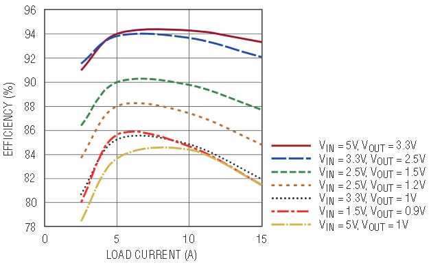
Figure 3. LTM4611 efficiency vs load current for various input and output voltages.
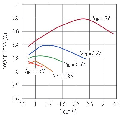
Figure 4. LTM4611 power loss at full load for various input and output voltages.
For an increasing number of applications, reducing power loss at light loads is as important—if not more important—than reducing power loss at heavy loads. Digital devices are being increasingly, deliberately designed to operate in lower-power states for as long as possible and whenever practical (for energy conservation), and draw peak power (full load) only intermittently. Figures 5 and 6 show the efficiency benefits of operating in PSM and Burst Mode operation at lighter load currents (<3A).
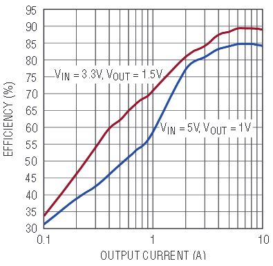
Figure 5. LTM4611 pulse-skipping mode efficiency.
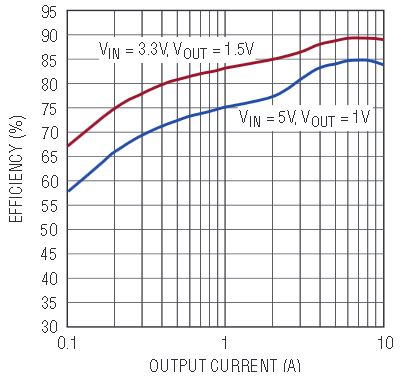
Figure 6. LTM4611 Burst Mode operation efficiency.
Thermally Enhanced Packaging
The device’s LGA packaging allows heat-sinking from both the top and bottom, facilitating the use of a metal chassis or a BGA heat sink. This form factor promotes excellent thermal dissipation with or without airflow. Figure 7 shows an infrared (IR) thermal image of the top of the LTM4611 demonstrating a power loss of 3.5W with no airflow, tested on a lab bench, converting a 5V input to a 1.5V output at 15A. The hottest surface temperature measures around 65°C.
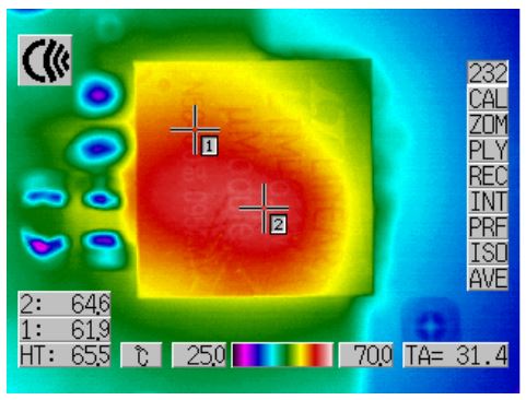
Figure 7. Top thermal image of an LTM4611 regulator producing 1.5V at 15A from at 5V Input. Power loss is 3.5W. No-airflow bench testing results in a 65°C surface temperature hotspot.
In contrast to Figure 7, Figure 8 shows an IR thermal image of the top of the LTM4611 demonstrating a power loss of only 3.2W with no airflow, tested on a lab bench, converting a 1.8V input to a 1.5V output at 15A.
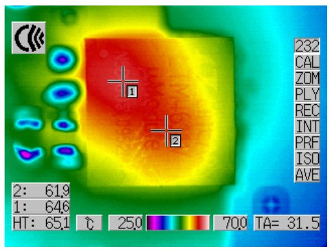
Figure 8. Top thermal image of an LTM4611 regulator producing 1.5V at 15A from at 1.8V Input. Power loss is 3.2W. No-airflow bench testing results in a 65°C surface temperature hotspot.
Hotspot locations, not their magnitude, are slightly changed from the positions seen during operation at 5V input.
At a low input voltage of 1.8V, conventional monolithic power IC solutions would struggle to deliver satisfactory gate drive amplitude to the power MOSFETs; one’s expectations of thermal performance would be lower than what the LTM4611 is able to deliver in Figure 8, thanks to its internal micropower bias generator.
Conclusion
The LTM4611 is a μModule buck regulator that easily fits into point-of-load applications needing high output current from low voltage inputs—down to 1.5V. Efficiency and thermal performance remain high across the entire input voltage range, simplifying placement in POL applications.
About the Authors
Alan Chern is a former associate design engineer at Linear Technology (now part of Analog Devices). He was responsible for supporting uModule® Power products in design, testing, demo board production, and product evaluatio...


