Minimizing Noise in High-Current Applications Using Tiny µModule® Regulators

Minimizing Noise in High-Current Applications Using Tiny µModule® Regulators
Sep 13 2026
Key Takeaways
|
Abstract
There is a growing need for power devices that are extremely clean for noise-sensitive applications like test and instrumentation, RF signal chain applications, medical diagnosis, and imaging systems that not only require low noise but also high output current and high efficiency. Traditional methods of using low-dropout regulators (LDOs) followed by switching regulators are increasingly challenged by the need for higher currents, better efficiency, and compact size solutions.
Introduction
Conventional step-down switching regulators have several sources of noise that affect low-frequency (<100kHz) performance. Most critical noise sources include feedback voltage reference, error amplifier, noise from the resistor divider used to set the output voltage, and noise gain created by this resistor divider. Many applications employ low-dropout regulators (LDOs) at the output of switching regulators to improve the noise performance. This switcher plus LDO solution results in increased total size and lower total efficiency and is limited in the output current capability of the LDO.
Analog Devices µModule switching regulators based on ADI’s Silent Switcher® 3 architecture utilize the current-reference derived feedback voltage architecture, which requires only one resistor to set the output voltage instead of top and bottom feedback resistors in conventional switching regulators.
This single resistor, along with the internal precision current source, sets the output voltage. This scheme allows unity gain over the output voltage and ensures low noise over the entire output voltage range. In addition to the current reference architecture, electromagnetic interference (EMI) noise cancellation technology techniques and proprietary design and packaging techniques are integrated in ultra-low-noise µModule regulators. The LTM4707, for example, further helps to improve the output noise performance of the switching regulators, especially low-frequency noise performance (10Hz to 100kHz frequency range).
To better understand ultra-low-noise measurements for power applications, this article highlights some of the noise measurement terminologies, discusses how to perform low-noise measurements, and provides reference noise measurements for the LTM4707 µModule Silent Switcher 3-based switching regulator and other modules for comparison.
Noise Measurement Setup
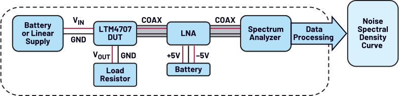
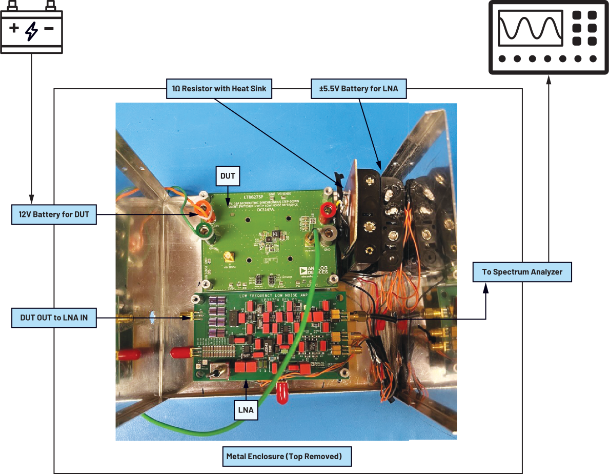
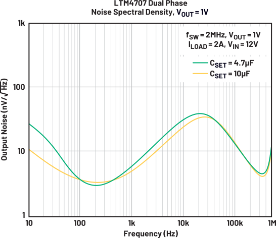
The noise measurement setup block diagram in Figure 1 shows the main components used for low-noise measurement for this article. Starting from the left, the battery or low-noise linear power supply provides cleaner power supply options for the device under test (DUT) and low-noise amplifier (LNA). The LNA provides necessary amplification of the DUT output signal for the intended frequency range only. The load resistor bank using a power resistor is preferred over an electronic load for further minimizing the interference due to test setup noise. Finally, the output from the LNA goes to the spectrum analyzer to measure the noise spectral density. Figure 2 shows an actual test setup, and Figure 3 shows an example measurement for the LTM4707 in dual-phase configuration.
Noise Terminology
Noise Spectral Density: Noise spectral density in V/√Hz is a way to represent wideband noise in a switching regulator over a given frequency range. This measurement shows the amplitude of the noise over the selected resolution frequency bandwidth.
RMS Noise: Root mean square noise parameter is the noise spectral density measurement integrated over the given frequency range, typically in µV rms over a given frequency range—for example, 10Hz to 100kHz frequency. This measurement allows a quick metric for comparison with other LDOs and switchers.
Spot Noise: Spot noise is the noise spectral density amplitude in V/√Hz for a given frequency data point. For example, the LTM4707 has spot noise of 4nV/√Hz at 1kHz frequency. This measurement is another quick metric for comparison with other LDOs and switchers.
Data Processing
To obtain noise spectral density in V/√Hz from the spectrum analyzer’s dBm measurement, Equation 1 is used.
Assuming spectrum analyzer is 50Ω terminated

where dBm is dB measurement relative to 1mW from the spectrum analyzer and RBW is the resolution bandwidth of the spectrum analyzer.
Equation 1 provides noise measurement at the output of the LNA. To obtain the noise measurement at the DUT, factor the LNA gain over the frequency range. For example, if the gain of the LNA is 1000× (60dB) at 100kHz, then the noise measurement from Equation 1 is divided by 1000 at 100kHz and so on for every frequency data point. Low noise amplifier gain can be measured using a waveform generator and a scope to measure the input and output signals of the LNA. For more accuracy, a network analyzer like Bode 100 can be used to measure LNA gain over the frequency range using a reference signal generated by the network analyzer.
To accurately measure noise from the DUT only, it is important to account for test setup noise. It is possible to isolate the noise coming from the LNA and spectrum analyzer by terminating the input of the LNA with a low-impedance resistor like 50Ω and performing a similar noise measurement with this setup as described. DUT noise can then be obtained by subtracting the setup noise from the total noise measured from the setup in Figure 1.
Further, once the noise spectral density measurement is available in V/√Hz, integrated RMS noise can be calculated for the selected frequency range. This can be obtained by graphically integrating the data using one of the methods like midpoint Riemann sum. Mathematical representation for this method is shown in Equation 2. Basically, it takes the average of adjacent data points and multiplies this average noise by the change in frequency between the adjacent data points and finally takes the square root of the sum of all the calculated data points.

where Nn is spectral noise density in V/√Hz and fn is the frequency in Hz.
LTM4707 Dual Phase
To extend the output current range of a switching converter without compromising noise performance, low-noise µModule regulators like the LTM4707 can be configured in a dual-phase configuration to support a total output current of 32A.
This µModule regulator utilizes peak current-mode control, which allows easy current sharing when operating in multiphase configuration. Tying multiple devices not only increases the output current capability but also provides much lower output noise. The schematic diagram in Figure 4 shows how to configure the LTM4707 in dual-phase configuration. Mainly VOUT, COMP, and SET pins of the two phases are tied together and CLKOUT of phase 1 is fed into the SYNC pin of phase 2. PHMODE is set to GND to separate the clock signal phase of both phases by 180° for best dual-phase interleaving.
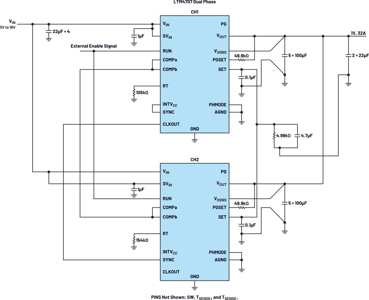
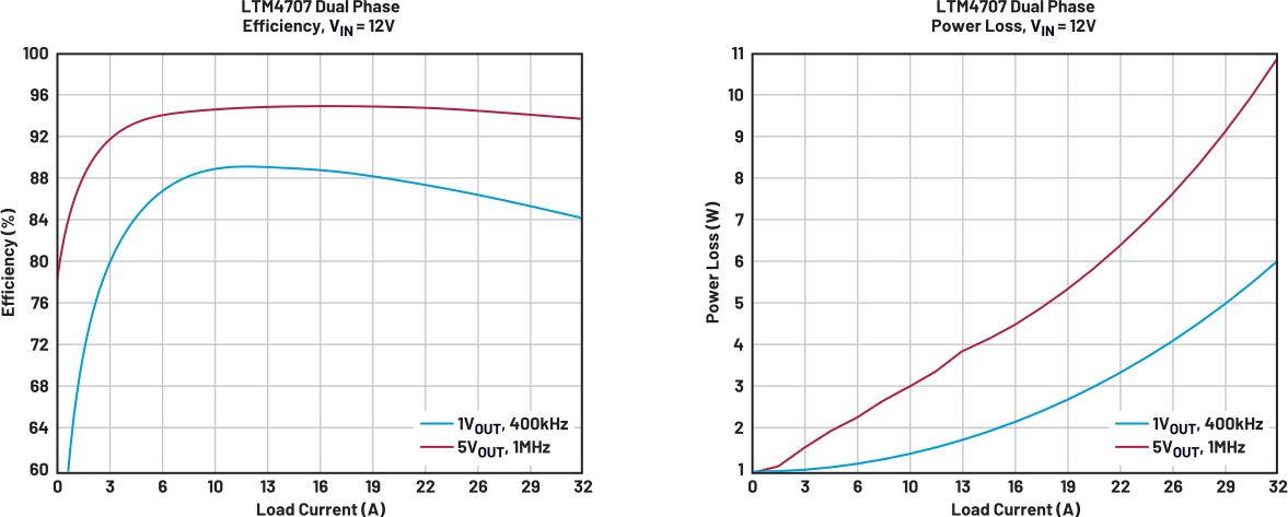
Figure 3 shows the noise spectral density results for two devices in dual-phase configuration. Efficiency and power loss for dualphase devices are also shown for reference in Figure 5.
LTpowerAnalyzer™ to Measure Noise Spectral Density
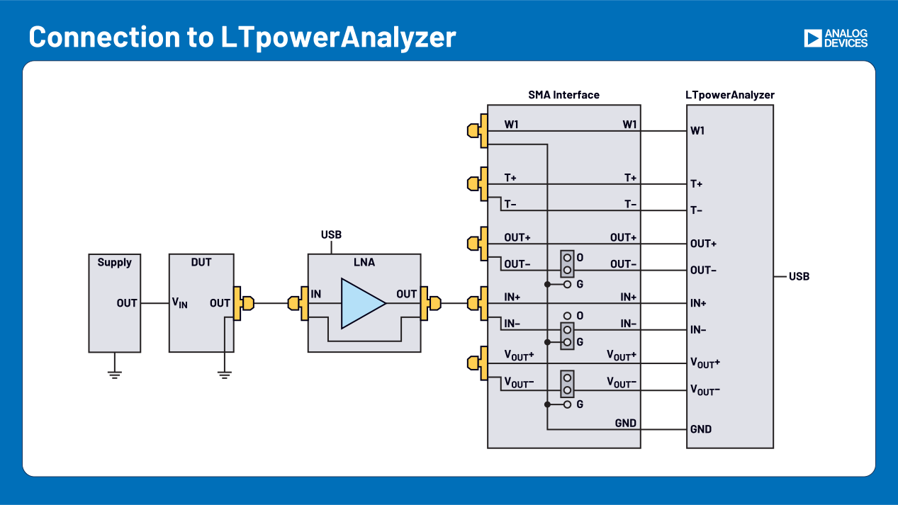
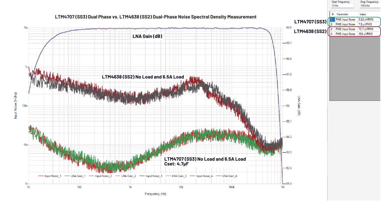
ADI’s LTpowerAnalyzer solution, along with the LNA unit, greatly simplifies the ultra-low-noise spectral density measurement. This solution allows for ultra-low-noise measurements without requiring an expensive spectrum analyzer or network analyzer. It also automates the final noise spectral density curve plotting and rms noise measurement calculations considerably, saving required test time and avoiding manual errors with the traditional spectrum analyzer test setup. Figure 6 shows the LNA, ADALM2000, LTpowerAnalyzer noise measurement setup, and Figure 7 shows the noise measurement results using the LTpowerAnalyzer solution comparing noise performance of the Silent Switcher 3 LTM4707 dual-phase solution vs. the Silent Switcher 2 LTM4638 dual-phase solution.
Conclusion
The noise performance of switching regulators can greatly impact noise-sensitive loads in end applications. In some cases, the noise performance of the switching converter may also make it difficult to pass stringent EMI emissions. With a conventional buck converter, low-frequency noise performance is a concern that increases with the output voltage due to the gain introduced by the resistor divider in the output voltage feedback network. Adding an LDO followed by a switching regulator increases cost, total solution size, and compromises efficiency. The LTM4707’s Silent Switcher architecture with current source reference for feedback voltage, advanced EMI noise mitigation design, and packaging techniques ensures ultra-low-noise performance (8µV rms integrated noise in 10kHz to 100kHz frequency range and <4nV spot noise at 1kHz frequency) along with high efficiency (~95% at 5VOUT, 16A IOUT).
References
Owen, Todd and Amit Patel. “AN-159: Measuring 2nV/√Hz Noise and 120dB Supply Rejection on Linear Regulators.” Analog Devices, Inc., February 2016.
Williams, Jim and Todd Owen. “AN-83: Performance Verification of Low Noise, Low Dropout Regulators.” Analog Devices, Inc., March 2000.
Zhang, Henry. “AN-149: Modeling and Loop Compensation Design of Switching Mode Power Supplies.” Analog Devices, Inc., January 2015.
About the Authors
Umit Shah is a senior design engineer for power modules with Analog Devices. He received his B. Tech degree in electronics engineering from Veermata Jijabai Technological Institute (University of Mumbai) and M.S. in
George (Zhijun) Qian is a senior design manager for power modules with Analog Devices. He is responsible for all LTM80xx products and some LTM46xx/LTM47xx products. He obtained his B.S. degree and M.S. degree from Zhejiang
Henry Zhang is an ADI fellow. He received a B.S.E.E. degree from Zhejiang University, China in 1994 and his M.S. and Ph.D. degrees in electrical engineering from Virginia Polytechnic Institute at State University,
Related to this Article
Products
RECOMMENDED FOR NEW DESIGNS
16VIN, 16A Ultralow Noise Silent Switcher 3 μModule Regulator
RECOMMENDED FOR NEW DESIGNS
20VIN, 15A Step-Down DC/DC µModule Regulator
EVAL-LTPA-KIT | Low-cost, High Performance, Compact Laboratory Tool for Evaluating and Characterizing Power Su...