Micropower SOT-23 Boost with Integrated Schottky Diode Provides Output Disconnect and Short Circuit Protection
Micropower SOT-23 Boost with Integrated Schottky Diode Provides Output Disconnect and Short Circuit Protection
Sep 1 2003
Introduction
The LT3464 is the only micropower boost converter in the industry to combine a 36V NPN power switch, power Schottky diode, and output disconnect into an 8-lead ThinSOT. This unprecedented level of integration saves several external components while offering true output disconnect, making it possible to generate outputs of up to 34V with a zero current shutdown while using a mere 40mm2 of board area (refer to Fig. 1).
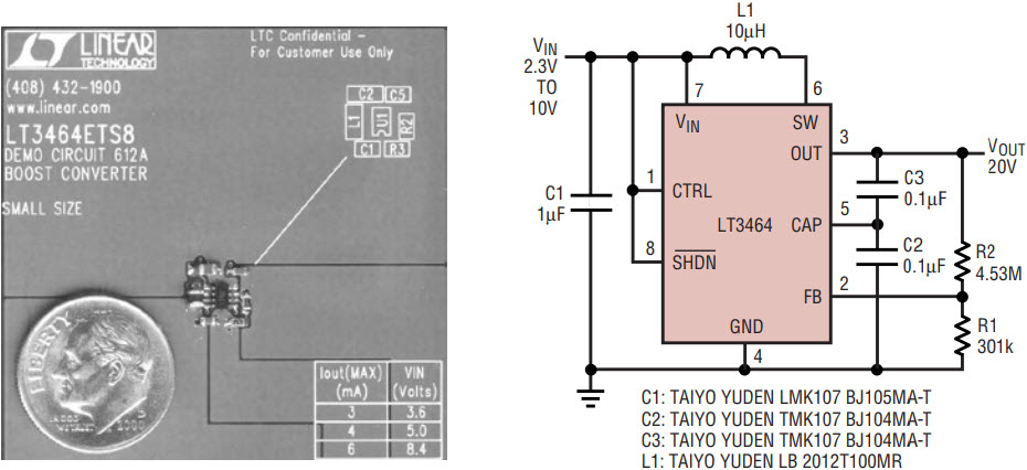
Figure 1. The integrated Schottky diode and output disconnect transistor result in a tiny solution occupying as little as 40mm2.
In addition to component savings, the LT3464 offers a low typical switch current limit of 115mA and fast switching, a combination that allows the use of a tiny chip inductor and tiny ceramic capacitors. The LT3464 also features Burst Mode control (see Figure 2), which results in highly efficient operation over a wide range of load currents and a low quiescent current of only 25µA typical. The CTRL pin of the LT3464 acts much like a dial on a lab power supply—it allows the output voltage to be varied, which is useful in applications for purposes such as LCD contrast adjustment.
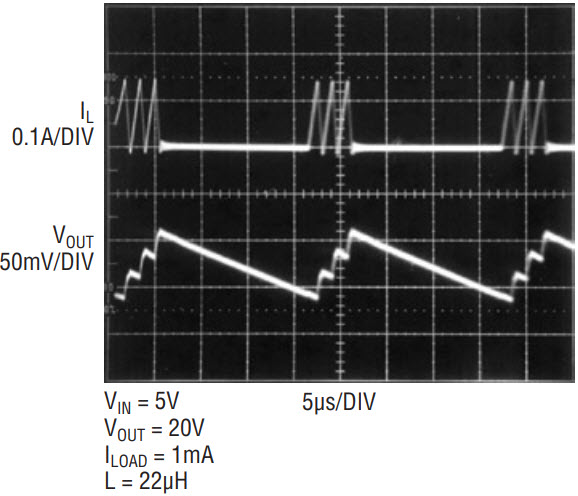
Figure 2. Burst Mode waveforms showing low output ripple. The LT3464 consumes only 25µA typical when not switching.
The LT3464’s small size and high efficiency make it an especially attractive power solution for portable electronics requiring long battery life and compact circuitry. See Figure 3 for a simplified block diagram of the LT3464.
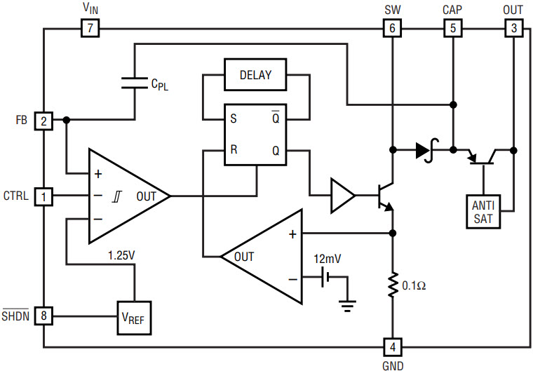
Figure 3. LT3464 block diagram showing integrated NPN switch, Schottky diode and output disconnect PNP.
Output Disconnect
In a simple boost circuit (Figure 4) there exists a DC path from the input supply (VIN) through the inductor and diode to the load (VOUT), effectively leaving the load connected to VIN during shutdown. The resulting current drain during shutdown is unacceptable in many applications, requiring the addition of several external components to isolate the load from VIN. To save space and complexity, the LT3464 is equipped with a PNP that completely disconnects the load from the Schottky diode during shutdown (see Figures 4 and 5). During normal operation, the control circuitry turns on the PNP and keeps it just out of saturation, resulting in low VCE(SAT) and low quiescent current. In addition, the disconnect circuit has a built in current limit of 25mA to protect the chip during a short-circuit at the output. This feature allows the LT3464 to tolerate an indefinite short, but care must be taken to avoid exceeding the maximum junction temperature.

Figure 4. A simple boost circuit with LT3464’s output disconnect allows the complete solution to draw less than 0.5µA during shutdown. The output disconnect is designed with a 25mA current limit to protect the circuit during short circuit conditions.
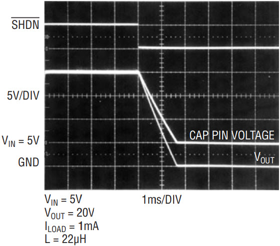
Figure 5. The output disconnect isolates the output load from the input supply during shutdown. CAP Pin voltage is the output of the Schottky in Figure 4.
Using the CTRL Pin
The LT3464 features an auxiliary reference input that provides an easy way to vary the output voltage for purposes such as LCD contrast adjustment or display dimming. When the CTRL pin held at or above 1.25V, the LT3464 uses the internal 1.25V reference, but when a voltage lower than 1.25V is applied to the CTRL pin, that voltage becomes the new reference. Figure 6 shows the output voltage versus the CTRL pin voltage for a 20V output circuit. Note that the LT3464 will not regulate the output to a voltage lower than the input.
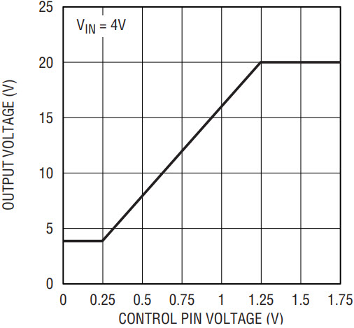
Figure 6. Using the CTRL Pin as an auxiliary reference input to control the output voltage.
LT3464 ±20V Dual Output Converter
Figure 7 shows a single-inductor dual-output converter for applications that require both a positive and negative voltage. The positive output is generated by a simple boost set up, whereas the negative output is generated using an inverting charge pump. Although well regulated, the negative output will have a slight offset from the positive output because the external diodes have a different on voltage when compared to the integrated Schottky diode.
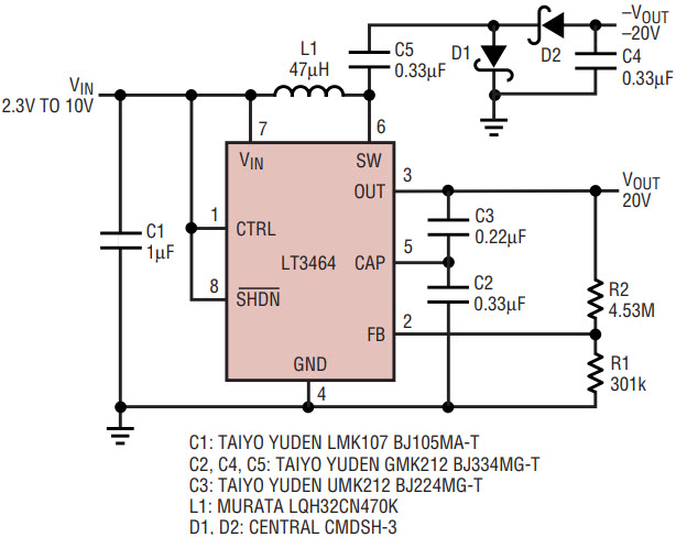
Figure 7. ±20V Dual output converter.
1-Cell Li-Ion to 16V Boost Converter
Figures 8 and 9 show that the LT3464 performs well in applications that need a high output voltage at a relatively low current. As shown in Figure 9, high efficiency is maintained with low output currents.
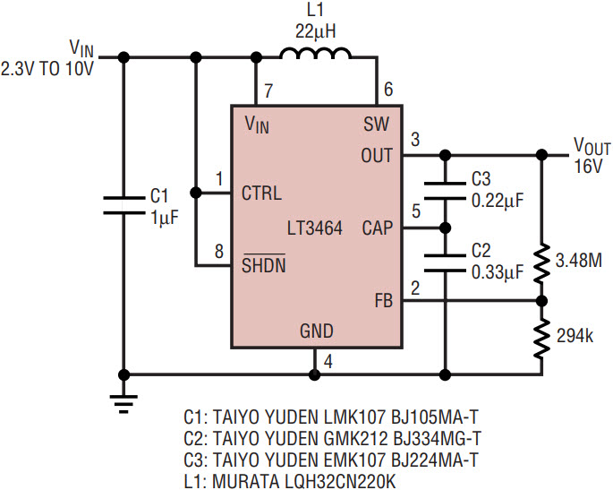
Figure 8. Li-Ion to 16V boost converter.
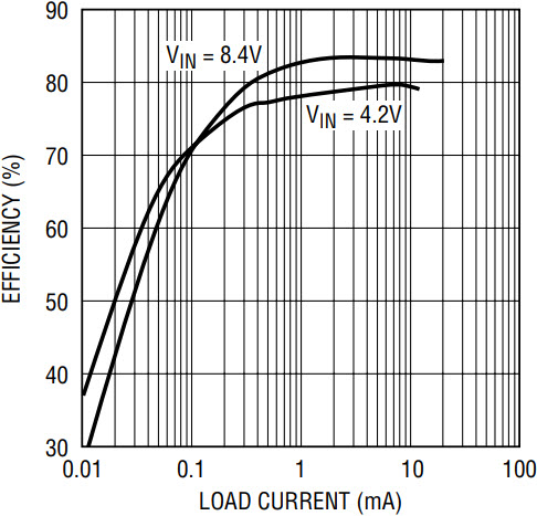
Figure 9. Efficiency for the circuit in Figure 7.
Conclusion
The LT3464 in the ThinSOT package produces an ultra compact boost solution featuring high efficiency, low quiescent current, true output disconnect, and low external parts count.


