Abstract
DATACLK output edge accuracy is highly dependent on the phase noise of the input CLK signal. DATACLKP/N is derived from the CLKP/N input and thus contributes a minimum amount of additional jitter or duty cycle error to the overall fidelity of the system. This document details the setup and hold timing specifications for the MAX19693 and the lab measurement of its total peak-to-peak jitter.
Introduction
System timing analysis typically employs additive jitter calculations to ensure that proper bus timing is met over temperature, voltage, and process variations. Clock signals derived from other signals exhibit duty-cycle distortion and increased jitter. Clock rates in the gigahertz range increase the impact of these additive timing errors.
The MAX19693 operates with a clock frequency up to 2GHz. It divides the input CLK to create the DATACLK signal used to synchronize the upstream digital source. Small timing variations of the DATACLK signal can cause the data interface to violate the setup and hold timing specifications. Accurately quantifying these errors enables a more robust system design.
DATACLK Output and DATA Input Timing
The negative hold time for the MAX19693 has the effect of collapsing the sampling window prior to the sample edge. However, having a negative hold time does not preclude using a longer or positive hold time, it simply means the sampling happens very early after setup. The hold time can be longer, and the designer must ensure they do not violate the subsequent setup time requirements.
The DAC has several internal clocks with various propagation delays that dictate the tSETUP and tHOLD specifications relative to the DATACLK output signal. The MAX19693 also supports double-data-rate (DDR) and quad-data-rate (QDR) digital input rates. With either DDR or QDR mode, the internal clocking system runs faster than DATACLK. In this case, the internal CLK is sampled every even-clock rising edge, while the DATACLK output is transitioned off every odd-clock rising edge. The internal workings of the data system are often obscured, but they should not be an issue as long as the end user follows the timing specifications.
DATACLK Output Function
The DATACLK is a differential LVDS signal used to synchronize the source data (FPGA) with the DAC input clock for proper sampling alignment at high speeds. An internal signal, derived from the DAC input clock, is used to latch the digital data received on the four, 12-bit, LVDS input ports: DAP/N[11:0], DBP/N[11:0], DCP/N[11:0], and DDP/N[11:0]. In order to properly time-align the input data port signals, a version of this internal latching clock is provided as an output signal for the user (DATACLK). The DATACLK can be configured as either a DDR signal that uses both the rising (0° phase) and falling (180° phase) edges of the DATACLK to synchronize the latching of input data, or as a quad-data-rate (QDR) that uses rising (0° phase), rising + 90°, falling (180° phase), and falling + 90° to latch the DAC input data.
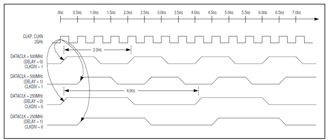
The LVDS DATACLKP/DATACLKN (DATACLK) output signals are derived from the CLKP/CLKN (CLK) input DAC clock through a basic D flip-flop (divide-by-2 or divide-by-4) and buffer circuit. Since the DATACLK output signal is derived from the CLK input signal, any jitter on the input clock will be translated to the output clock with the addition of a systematic jitter error caused by the internal buffering and clock domain circuitry. This jitter “adder” is the value that was investigated.
DATACLK Jitter and Duty Cycle Error – Lab Analysis
Three methods were used to measure the DATACLK and CLK jitter in order to extract the duty cycle error and the jitter “adder” of the DATACLK.
The first effort was made with an Agilent®/Keysight® Infiniium® DSA91304A (13GHz, 40Gsps) digital signal analyzer using both a standard 50? input and a differential probe (7GHz, Agilent 1134A). Measurements of the input DAC CLK demonstrated larger than expected jitter values for the Rohde & Schwarz® SMF100A signal generator. It was subsequently determined that the specified sampling error for the digital signal analyzer (DSA) was ~17mV in the 500mV range, resulting in a best-case jitter measurement capability of ~12ps peak to peak (~12psP-P). The DSA was performing better than that, at ~6psP-P, but this would not provide the overall measurement capability required for answering the DATACLK jitter question.
A second attempt was made with a Tektronix® Tek 11801C digital sampling oscilloscope (DSO) using both a 50? sampling head (SD-26) and a high-impedance sampling head (SD-14). Unfortunately, the trigger method used for the Tek DSO requires a version of the input signal to be connected to the trigger input commonly with a power splitter and a delay line (DL-11). Because the DATACLK is a divided-by-4 version of the input clock, sampling edges resulted in eye-diagram-like traces. The Tek 11801C does not have high-level jitter analysis and the histogram functions were not providing reliable measurement results (on the order of 40psP-P jitter for the input clock source).
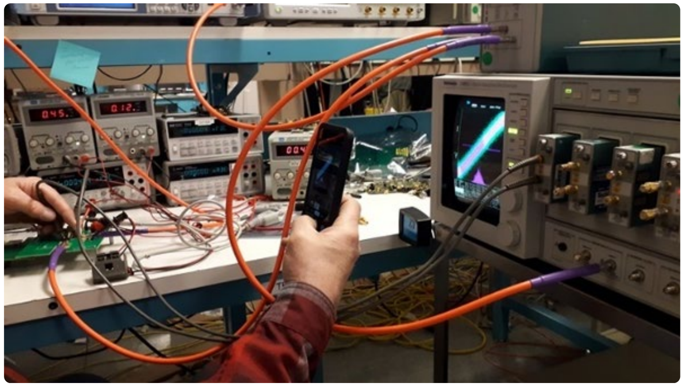
The final method using a Tektronix DPO72304SX digital phosphor oscilloscope (DPO) to measure DATACLK jitter was successful.
Lab Setup
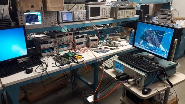
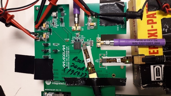
The MAX19693EVKIT was used for measuring jitter. The evaluation kit (EV kit) was connected to a Xilinx® VC707 FPGA evaluation system through an FPGA Mezzanine Card (FMC) adaptor to provide input data to the MAX19693 RF DAC. A Rohde & Schwarz SMF100A signal generator was configured for a 2.000GHz, +15dBm output as the CLK source to a MAX19693EVKIT connected to the CLK SMA. The EV kit was powered from two lab supplies—one providing 1.8V to both VDD and AVCLK, and the second at 3.3V for AVDD. A Tektronix DPO72304SX DPO was used to measure both the CLK input and DATACLK output jitter values. The input CLK signal was connected to a Tek P7713 differential probe after the triple transformer network on the EV kit board. Similarly, another P7713 differential probe was connected to the DATA-CLKP/N output signal at the R2, R3 output taps on the EV kit. The Tek DPO was configured to trigger the signal of interest and set up to measure the jitter with the “One Button Jitter” setup for both the CLK input and DATACLK output signals.
Lab Results
Assessment of both the DAC clock input jitter and the data clock output jitter could take several different forms. The Tek DPO has built-in analysis algorithms to measure time interval error (TIE), total jitter (TJ), random jitter (RJ), and deterministic jitter (DJ). Given that both signals should be periodic and essentially a fixed frequency/data rate, any one of these methods should provide an indication of the jitter ‘added’ to the system by the MAX19693.
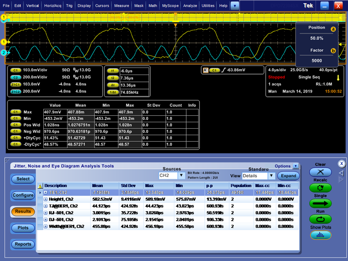
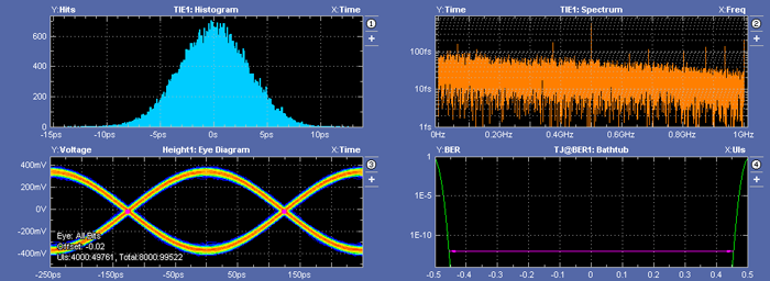
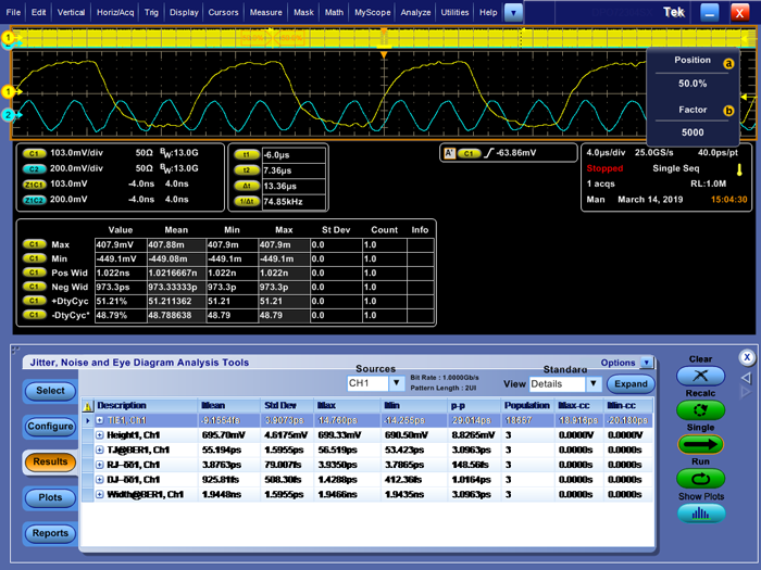
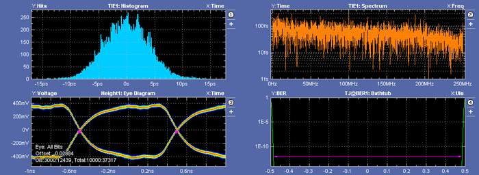
The following tables provide a summary of three data sets collected and the resulting values for the input CLK and the output DATACLK jitter measurements:
| Sample | TIEP-P | TJP-P | RJP-P | DJP-P |
| CLK 1 | 26.6ps | 601fs | 51fs | 106fs |
| DATACLK 1 | 29.0ps | 3.1ps | 149fs | 1.0ps |
| CLK 2 | 26.6ps | 601fs | 66.8fs | 727fs |
| DATACLK 2 | 29.0ps | 4.2ps | 275fs | 1.0ps |
| CLK 3 | 26.6ps | 788fs | 66.8fs | 727fs |
| DATACLK 3 | 32.1ps | 5.7ps | 275fs | 2.9ps |
Directly subtracting the input peak-to-peak jitter from the output peak-to-peak jitter resulted in a delta or total ‘added’ jitter from the MAX19693. This ‘added’ jitter included components of the duty cycle error and the systematic jitter, as shown in Table 2.
| Sample | TIEP-P | TJP-P |
| Sample 1 | 2.4ps | 2.5ps |
| Sample 2 | 3.3ps | 3.6ps |
| Sample 3 | 5.5ps | 4.9ps |
| Samples Average | 3.7ps | 3.7ps |
These three samples were averaged to find a typical value of 3.7ps for the total ‘added’ peak-to-peak jitter.
DATACLK Jitter – Simulation
Simulation results were run using power supply transients of 100mV amplitude and a 10ps pulse width, and 1ps rise/fall times at a period of 500ps with +Ve and -Ve staggered by 250ps. The simulation options included a no-noise option, a transient noise option, and a power supply noise train with ‘creep’ (10ps every cycle), which provided an asynchronous power supply noise result. The simulation with creep was a 300ns run, with noise beginning at 100ns and continuing through the end at 300ns, thus allowing about 100 cycles of a 500MHz clock across the 200ns noise window.
| Simulation | Min | Max | JP-P | s |
| No Noise | -5.7fs | 10.8fs | 16.5fs | 3.3fs |
| Transient Noise | -9.6fs | 14.4fs | 24.0fs | 5.4fs |
| Power Supply Noise Creep | -1.56ps | 2.12ps | 3.68ps | 0.84ps |
Conclusion and Recommendation
Review and analysis of the internal circuity provided a conservative estimate of 2~4ps for the DATACLK output jitter ‘added’ to the CLK input. Further simulation and actual lab measurements both indicated a peak-to-peak jitter value of approximately 3.7ps. Based on these results, Maxim recommends a conservative number of 4ps for the MAX19693 DATACLK ‘added’ output jitter for use in timing budget calculations.


